Reasons for choosing our testing services
ZHONGXI Testing has obtained inspection qualification certifications from multiple countries and regions worldwide. We possess a senior testing team and advanced testing methods, providing independent, impartial, and professional third-party verification services for global carbon projects.
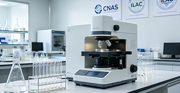
Internationally recognized authority
Certified by multiple international standards such as CNAS, VCS, and GS, with reports universally applicable worldwide.

Global service capability
Covering 140+ countries and regions, it supports on-site detection and remote verification in multiple languages.
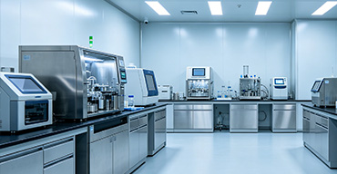
Professional experimental methods
Adopt standard experimental methods to ensure accurate and reliable data.
Semiconductor Material Testing Services: Precision Analysis for Wafer, Substrate & Device Manufacturing
As an independent third-party testing service provider, we support semiconductor manufacturers, wafer foundries, material suppliers, packaging houses, and R&D institutions in verifying the quality, purity, and performance of semiconductor materials. Semiconductor materials – including elemental semiconductors (silicon, germanium), compound semiconductors (GaAs, InP, GaN, SiC), and advanced substrates (SOI, sapphire, diamond) – require extreme levels of cleanliness, crystallographic perfection, and electrical uniformity. Our accredited laboratory performs a full range of physical, electrical, chemical, and structural characterisation tests according to global standards (SEMI, ASTM, ISO, JIS, GB). This article outlines our semiconductor material testing capabilities – including scope, key test items, and standard test methods – to help you select the right analytical services for your wafers, epi-layers, or device structures.
1. Our Testing Scope for Semiconductor Materials
We cover virtually all types of semiconductor materials and product forms:
By material type: Elemental semiconductors – silicon (single crystal, polycrystalline, amorphous), germanium; Compound semiconductors – III-V (GaAs, InP, GaSb, InAs, GaN), II-VI (CdTe, ZnSe, ZnO), IV-IV (SiC, SiGe); Oxide semiconductors – ITO, IGZO; Wide bandgap materials – SiC, GaN, diamond, AlN; Organic semiconductors; 2D materials (graphene, MoS₂) upon request.
By product form: Bulk wafers (as-cut, lapped, polished, epitaxial), ingots and boules, reclaimed wafers, test wafers, thin films (deposited or grown), epitaxial layers, junction structures, and die-level samples.
By industry application: Integrated circuit (logic, memory, analog) manufacturing; Power electronics (SiC, GaN); RF and microwave devices; Optoelectronics (LEDs, laser diodes, photodetectors); MEMS and sensors; Photovoltaics (Si, CdTe, CIGS); Research and prototyping.
2. Key Test Items We Perform
Our semiconductor testing services are grouped into seven main categories. Each category addresses specific quality, performance, and reliability requirements.
2.1 Physical & Dimensional Characterisation
Wafer thickness, total thickness variation (TTV), bow, warp – critical for lithography and handling.
Flatness (global, local, site flatness – SFQR) – for depth of focus in steppers.
Edge profile and edge roll-off – prevents chipping and slip.
Surface roughness (Ra, Rq, Rmax) – by stylus profilometer or atomic force microscopy (AFM).
Particle count and size distribution – for cleanroom wafer qualification.
Crown, taper, and notch geometry – for wafer alignment.
2.2 Crystallographic & Structural Analysis
Crystal orientation (primary and secondary flat) – verified by X-ray diffraction (XRD) or Laue back-reflection.
Resistivity (bulk and sheet) – four-point probe and eddy current.
Dopant type (n-type vs. p-type) – hot probe or Seebeck effect method.
Majority carrier concentration (extracted from resistivity vs. calibration curves).
Dislocation density (etch pit density – EPD) – for silicon and compound semiconductors.
Stacking fault and microdefect evaluation – by optical microscopy after preferential etching.
Crystal perfection (X-ray rocking curve – FWHM) – for epitaxial layers.
Grain size and boundary analysis (polysilicon, sintered materials).
2.3 Electrical Properties
Resistivity (bulk) – four-point probe (ASTM F43).
Sheet resistance – van der Pauw or linear four-point probe for thin layers.
Carrier concentration and mobility (Hall effect) – van der Pauw configuration (ASTM F76).
Minority carrier lifetime (photoconductance decay, µ-PCD) – for bulk silicon.
Capacitance-voltage (CV) profiling – for doping profile in epitaxial layers.
Breakdown Voltage, Leakage Current – for power device substrates.
Contact resistance (TLM, CTLM) – for metallisation evaluation.
Dielectric strength of insulator layers (oxide, nitride).
2.4 Chemical & Trace Analysis
Total carbon and oxygen content (by FTIR) – in silicon wafers (interstitial oxygen, substitutional carbon).
Metal contamination (surface or bulk) – ICP-MS, TXRF, VPD-ICP-MS (e.g., Fe, Cu, Ni, Al, Cr, Na, K).
Anion and cation analysis (ion chromatography) – for cleaning bath validation.
Surface organic residues (contact angle, TXRF).
Bulk purity (by GDMS or ICP-MS) – for high-purity silicon and compound feedstocks.
Dopant concentration (by SIMS) – depth profiling of B, P, As, Sb, Al, Ga, etc.
Residual gas analysis (RGA) – for outgassing from materials.
2.5 Surface & Interface Characterisation
Surface roughness (AFM, optical interferometry).
Surface contamination (TXRF, XPS, ToF-SIMS).
Native oxide thickness (ellipsometry, XPS).
Flatband voltage and interface trap density (C-V) – for MOS structures.
Adhesion of thin films (scratch test, tape test).
Surface wettability (water contact angle).
Defects (scratches, pits, orange peel) – by automated optical inspection (AOI).
2.6 Thermal & Optical Properties
Thermal conductivity – for SiC, GaN, and diamond substrates (laser flash or 3ω method).
Coefficient of thermal expansion (CTE) – by dilatometry.
Thermal diffusivity and specific heat.
Emissivity, reflectivity, transmittance (UV-VIS-NIR spectrophotometry).
Photoluminescence (PL) mapping – for bandgap uniformity and defect detection in compound semiconductors.
Raman spectroscopy (strain, crystalline quality, polytype identification for SiC).
2.7 Epitaxial Layer & Thin Film Characterisation
Layer thickness (FTIR, ellipsometry, SIMS, SRP).
Doping concentration profile (SIMS, ECV – electrochemical CV).
Morphology of epi-layers (Nomarski microscopy, AFM).
Particle density on epi-wafers.
Cross‑sectional TEM (for interface sharpness, defect analysis).
Composition of ternary or quaternary compounds (XRD, EDX).
3. Standard Test Methods We Apply
All tests are performed according to internationally recognised standards (SEMI, ASTM, ISO, JIS, GB). Our laboratory is ISO/IEC 17025 accredited with class 100 cleanroom facilities and advanced characterisation instruments.
3.1 Physical & Dimensional Methods
Wafer thickness, TTV, bow, warp: SEMI MF1530, ASTM F1390 (non‑contact capacitive or laser triangulation).
Flatness (SFQR): SEMI MF1530, ASTM F1530.
Surface roughness (profilometer): SEMI MF1811, ASTM D7127.
Particle count: SEMI MF1807, ISO 14644 (surface particle inspection by laser scattering).
Edge profile: SEMI MF1810.
3.2 Crystallographic & Resistivity Methods
Crystal orientation (XRD, Laue): SEMI MF26, ASTM E975.
Resistivity (four-point probe): SEMI MF84, ASTM F43.
Dopant type (thermoelectric method): SEMI MF42, ASTM F42.
Dislocation density (etch pit): SEMI MF1809 (silicon), ASTM F47 (GaAs).
X-ray rocking curve: ASTM F2065 (FWHM of epitaxial layers).
3.3 Electrical Test Methods
Hall effect and mobility: ASTM F76, SEMI MF76.
Minority carrier lifetime (µ-PCD): SEMI MF1535, ASTM F28.
CV profiling: ASTM F1392 (doping density in epitaxial layers).
Sheet resistance (van der Pauw): SEMI MF84.
Contact resistance (TLM): ASTM F1981.
3.4 Chemical & Trace Analysis Methods
Oxygen and carbon in silicon (FTIR): SEMI MF1188, ASTM F121.
Metal contamination (TXRF): SEMI MF1526, ISO 14706.
VPD-ICP-MS (vapor phase decomposition): SEMI MF1726, ASTM F1726.
Bulk purity (GDMS): ASTM F1593.
SIMS depth profiling (dopants): SEMI MF1635, ASTM F1635.
Ion chromatography for anions/cations: SEMI MF1342, ASTM D4327.
XPS (X-ray photoelectron spectroscopy): ASTM E995, E1523 – surface chemistry and oxide thickness.
Ellipsometry (film thickness, refractive index): SEMI MF576, ASTM E1453.
Contact angle measurement (wettability): ASTM D5946.
Scratch adhesion test: ASTM C1624.
3.6 Thermal & Optical Methods
Thermal conductivity (laser flash): ASTM E1461, ISO 22007-4.
CTE (dilatometry): ASTM E228.
UV-VIS-NIR spectrophotometry: ASTM E1348, SEMI MF1391.
Photoluminescence (PL) mapping: ASTM F2160.
Raman spectroscopy for strain/polytype: ASTM E1683, E3096.
3.7 Epitaxial Layer & Thin Film Methods
Epilayer thickness (FTIR): SEMI MF95, ASTM F95.
Doping profile (ECV – electrochemical CV): SEMI MF1445, ASTM F1445.
Cross‑sectional TEM (for interface, defects): ASTM E2112.
XRD for composition (e.g., AlGaAs, InGaAs): ASTM F2024.
4. Why Choose Our Third-Party Semiconductor Material Testing Services?
As an independent, non‑manufacturing laboratory, we provide unbiased, accurate, and confidential results. Our strengths include:
ISO/IEC 17025 accreditation – with CNAS/CMA marks, regularly participating in round-robin tests (e.g., SEMI, NIST).
Class 100 (ISO 5) cleanroom – for particle-sensitive characterisation and wafer handling.
Comprehensive instrument park – AFM, XRD, SEM-EDS, XPS, ICP-MS, SIMS, ECV, µ-PCD, FTIR, Hall effect system, four-point probe, ellipsometer, Raman, PL mapper.
Tailored sampling plans – from single-piece failure analysis to full lot monitoring.
Fast turnaround – typical 3-5 business days for routine wafer tests; rush options available.
Confidential data protection – NDA protected, secured data storage.
Consultative approach – we help you select the right test methods, understand specification limits (SEMI standards), and interpret results for process improvement.
Whether you need incoming wafer inspection, epitaxial layer qualification, contamination root‑cause analysis, or material release for device manufacturing, our semiconductor specialists are ready to support your quality assurance and R&D efforts.
Get Started with Your Semiconductor Testing Project
Contact our team with your material type (e.g., 200mm silicon, 150mm SiC, GaAs epi‑wafer), applicable standards (SEMI, ASTM, customer spec), and required test items. We will provide a detailed quotation, sample submission guidelines (including cleanroom packaging requirements), and a testing schedule. Let us help you achieve the highest levels of purity, uniformity, and performance for your semiconductor materials.
This article provides an overview of our semiconductor material testing capabilities. For specific test methods, sample quantity, and pricing, please request a tailored service proposal.