Reasons for choosing our testing services
ZHONGXI Testing has obtained inspection qualification certifications from multiple countries and regions worldwide. We possess a senior testing team and advanced testing methods, providing independent, impartial, and professional third-party verification services for global carbon projects.
Internationally recognized authority
Certified by multiple international standards such as CNAS, VCS, and GS, with reports universally applicable worldwide.

Global service capability
Covering 140+ countries and regions, it supports on-site detection and remote verification in multiple languages.

Professional experimental methods
Adopt standard experimental methods to ensure accurate and reliable data.
Comprehensive Characterization of Indium Tin Oxide (ITO) – Advanced Analytical Solutions for Compositional Precision, Trace Impurity Control, and Optoelectronic Property Verification
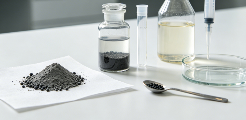
You are searching for indium tin oxide (ITO) detection because this transparent conducting oxide is critical for display panels (LCD, OLED), touch sensors, photovoltaic devices, and low‑emissivity glass. ITO performance is governed by far more than a simple In/Sn ratio; it depends on precise stoichiometry (In₂O₃/SnO₂ ratio), trace impurity levels (e.g., Fe, Cu, Pb, Cd), crystal structure (bixbyite phase, grain orientation), film thickness, sheet resistance, optical transmittance, and surface roughness. Routine elemental analysis (e.g., XRF for In and Sn alone) cannot reveal the critical dopant uniformity, trace contaminants, or the structural and electrical properties that directly affect device yield and reliability. You require a laboratory that delivers multi‑parameter, high‑resolution characterization integrating bulk composition, ultra‑trace impurity profiling, crystallinity and grain size, film electrical and optical performance, and surface morphology. Our facility provides exactly that: an ISO 17025‑accredited, fully validated analytical platform for ITO, compliant with SEMI, ASTM, and JIS standards, and covering both bulk materials (targets, sputtering feedstocks) and deposited thin films.
Analytical Framework – From Bulk Composition to Ultra‑Trace Impurity Mapping, Crystal Structure, and Functional Film Testing
We offer a tiered analytical strategy tailored to your quality control, process development, or failure analysis needs. Our platform includes:
• Major element composition (In₂O₃ and SnO₂) – X‑ray fluorescence (XRF) and ICP‑OES/ICP‑MS after digestion. Our primary method is wavelength‑dispersive XRF (PANalytical Zetium) on fused beads or pressed pellets, achieving repeatability of ±0.05% (absolute) for In₂O₃ and ±0.02% for SnO₂, which is the accepted reference for ITO target certification. For cross‑validation and for samples with low Sn content, we use ICP‑OES (Agilent 5110) after microwave digestion (HCl + HNO₃ + HF), providing simultaneous determination of In, Sn, and 30+ other elements with LOQs of 0.001–0.005%. For ultra‑trace toxic metals (Pb, Cd, As, Hg, Cr), we employ ICP‑MS/MS (Agilent 8900) with reaction cell, achieving sub‑ppm detection limits (0.01–0.1 mg/kg) as required for RoHS and REACH compliance.
• Trace impurity profiling (Fe, Cu, Ni, Zn, Al, Ca, Mg, etc.) – ICP‑MS and glow discharge mass spectrometry (GD‑MS). For the highest sensitivity (down to ppb level) and direct solid analysis, we offer GD‑MS (Thermo Scientific Element GD) – a technique that provides a full mass spectrum without acid digestion, eliminating contamination and dissolution issues. This is especially valuable for detecting elements that are difficult to dissolve or have high blank levels. We report quantitative concentrations of up to 70 elements with detection limits as low as 0.001 µg/g (1 ppb) for most metals.
• Crystal structure and phase purity – X‑ray diffraction (XRD) with Rietveld refinement. Using a PANalytical X’Pert Pro MPD with Cu Kα radiation, we identify the cubic bixbyite structure (In₂O₃) and detect any secondary phases (e.g., In₄Sn₃O₁₂, SnO₂, or metallic In/Sn). We perform Rietveld refinement to obtain lattice parameter (a), crystallite size, and microstrain – parameters that correlate with sputtering behaviour and film stress. We also quantify the degree of solid solution formation (Sn substitution in the In₂O₃ lattice) by analysing the peak shifts. Detection limit for secondary phases is 0.5 wt%.
• Thin film electrical and optical properties – four‑point probe, Hall effect, and UV‑Vis‑NIR spectrophotometry. For ITO coated substrates, we measure sheet resistance (Ω/□) by four‑point probe (Jandel RM3000) with accuracy ±1% over the range 0.1–10,000 Ω/□. We determine carrier concentration and mobility by Hall effect (Lake Shore HMS 7600), and we measure optical transmittance (300–2500 nm) using a PerkinElmer Lambda 1050 spectrophotometer with an integrating sphere, reporting average visible transmittance (400–700 nm) and near‑infrared reflectance – critical for display and solar cell applications. All measurements are performed on standard film stacks (glass or polymer) and meet ASTM F1529 and JIS R 1635.
• Surface morphology and film thickness – scanning electron microscopy (SEM), atomic force microscopy (AFM), and stylus profilometry. We provide high‑resolution SEM (Tescan MIRA3) with EDS for surface imaging and local composition mapping. For nanoscale roughness and step height, we use AFM (Bruker Dimension Edge) to obtain root‑mean‑square roughness (Rq) and average roughness (Ra) over areas from 1×1 µm to 50×50 µm. Film thickness is measured by stylus profilometry (Bruker Dektak XT) with a vertical resolution of 0.5 nm, and also by X‑ray reflectometry (XRR) for ultra‑thin films (< 50 nm).
• Thermogravimetric and thermal analysis – TGA‑DSC for sintering behavior and phase transitions. For ITO powder or green compact, we perform simultaneous TGA‑DSC (Netzsch STA 449) up to 1400°C in air or argon to characterise mass loss (volatiles, organics), sintering onset, and solid‑state reactions. This data is used to optimise target densification and to detect residual binders.
No other service integrates XRF, ICP‑MS, GD‑MS, XRD with Rietveld, four‑point probe, Hall effect, UV‑Vis‑NIR spectrophotometry, SEM, AFM, and TGA under one ISO 17025‑accredited system for ITO – delivering a complete quality profile from bulk composition to thin film functional performance.
Why Our Laboratory Is the Premier Partner for ITO Characterization
Our specialization in transparent conductive oxides and advanced electronics materials has enabled us to overcome the unique challenges of ITO testing: high In matrix causing spectral interferences in ICP (we use internal standards and matrix‑matched calibration), very low impurity limits (single ppm for many elements) requiring ultra‑clean handling and GD‑MS capability, difficulty in obtaining reproducible electrical measurements on thin films (we use calibrated probes and van der Pauw geometry), and the need for non‑destructive analysis of finished devices (we offer optical and X‑ray methods with no sample damage). Our distinct advantages include:
1. Multi‑technique cross‑validation for composition and stoichiometry. For each batch, we cross‑check In/Sn ratios from XRF, ICP‑OES, and (for powders) from the lattice parameter derived from XRD – ensuring an absolute accuracy of ±0.1% for Sn/(In+Sn).
2. Ultra‑trace GD‑MS capability with full element coverage. Our GD‑MS system is one of the few commercially available in the region, providing direct solid analysis without acid digestion – eliminating contamination risks and enabling detection of elements like C, N, O, and halogens that are difficult by solution methods. This is critical for detecting impurities that degrade electrical performance (e.g., Fe, Cu, Ni, Cr) at < 1 ppm levels.
3. State‑of‑the‑art thin film characterization under controlled environments. We perform electrical and optical measurements in a class 100 cleanroom with temperature and humidity control, ensuring reproducibility within ±2% for sheet resistance and ±0.5% for transmittance.
4. Comprehensive reference material and proficiency testing. We maintain certified ITO reference materials (NIST SRM 2062 and in‑house standards) and participate in ASTM Interlaboratory Studies for ITO, consistently achieving |z|‑score < 0.5.
5. ISO 17025 accreditation and global industry acceptance. Our methods comply with SEMI C3, ASTM E2371, JIS R 1635, and ISO 15318. Our test reports are accepted by display panel manufacturers, semiconductor foundries, solar cell producers, and glass coating companies worldwide.
Technical Depth – Beyond Basic Quality Indicators
While many laboratories report only In₂O₃/SnO₂ ratio and sheet resistance, we provide actionable insights for advanced process control:
• Impurity impact on electrical mobility. Using our trace impurity data combined with Hall effect mobility, we identify which specific contaminants (e.g., Fe or Cu) are most detrimental to carrier mobility, and we provide a “purity‑mobility index” – a predictive metric for sputtering performance.
• Grain orientation and film stress analysis by XRD. We perform pole figure analysis to determine the preferred orientation (e.g., (222) or (400)) of the ITO film, which influences etching behaviour and surface roughness. We also calculate residual stress from peak shifts using the sin²ψ method – critical for preventing cracking in flexible substrates.
• Depth profiling by GD‑MS and XPS. We offer sputter depth profiling to reveal compositional uniformity across the film thickness, detecting surface enrichments of Sn or In that may arise from deposition conditions.
• Correlation between target density and sputtering rate. By combining true density (He pycnometry) with XRD crystallite size and SEM porosity, we calculate a “sputtering yield predictor” that estimates erosion rate and target lifetime – a service unique to our laboratory.
Supporting Your Specific ITO Testing Objectives
Your search for ITO detection likely aligns with one or more of these scenarios. We provide precisely tailored solutions:
• Raw material acceptance for ITO target production. We test incoming In₂O₃ and SnO₂ powders as well as the final sintered targets for composition (In₂O₃/SnO₂ ratio), trace impurities (by GD‑MS), density, and phase purity (XRD). We issue a certificate of analysis (COA) with pass/fail judgement relative to your specification. Typical turnaround: 5‑7 working days.
• Process control for sputtering deposition. For ITO film producers, we analyse witness samples (glass or Si wafers) after each run to measure sheet resistance, thickness, transmittance, and composition (by EDS or XRF). We provide rapid feedback (24‑hour priority service) to fine‑tune oxygen partial pressure, power, and substrate temperature.
• Failure analysis for defective ITO films (high resistivity, low transmittance, poor adhesion). We perform comparative analysis between good and defective films, including SEM for microcracks, AFM for roughness changes, XPS for surface contamination (carbon or organic residues), and SIMS (optional) for depth profiling of trace contaminants. We identify the root cause – e.g., oxidation, carbon contamination, or non‑uniform Sn distribution – and recommend corrective adjustments.
• Regulatory compliance (RoHS, REACH, China RoHS). We provide full heavy metal declarations for Cd, Pb, Hg, Cr⁶⁺, PBBs, and PBDEs, with LOQs far below regulatory limits. We also test for halogen content (F, Cl, Br, I) by ion chromatography if required.
• Research and custom method development. For academic or industrial R&D, we offer customised characterisation including high‑temperature X‑ray diffraction (in‑situ), spectroscopic ellipsometry (for optical constants n and k), and temperature‑dependent Hall measurements. We also perform method validation and inter‑laboratory studies for novel ITO variants (e.g., IZO, IGZO).
Partner with Us for Definitive ITO Characterisation
Choosing our laboratory gives you access to a dedicated electronic materials analysis team with over 12 years of experience in transparent conductive oxides. We provide free sampling kits (pre‑cleaned, inert‑packaged containers for powders, and special holders for wafers or glass substrates), a detailed sampling protocol (to avoid contamination and damage), and direct consultation with our senior materials scientist for data interpretation. No project is too large or too small – from a single R&D film to routine quality control of high‑volume production targets.
Contact our technical team with your ITO testing requirements. We will provide a customised project quotation and, for qualifying clients, a free preliminary screening (composition by XRF and sheet resistance) on up to three samples. Your search for authoritative, high‑depth characterisation of indium tin oxide ends here – because we deliver the compositional, structural, electrical, and optical insight that routine single‑parameter tests cannot provide.