Reasons for choosing our testing services
ZHONGXI Testing has obtained inspection qualification certifications from multiple countries and regions worldwide. We possess a senior testing team and advanced testing methods, providing independent, impartial, and professional third-party verification services for global carbon projects.

Internationally recognized authority
Certified by multiple international standards such as CNAS, VCS, and GS, with reports universally applicable worldwide.

Global service capability
Covering 140+ countries and regions, it supports on-site detection and remote verification in multiple languages.

Professional experimental methods
Adopt standard experimental methods to ensure accurate and reliable data.
Comprehensive Multi‑Scale Characterization of Silicon Carbide Nanorods: A Specialized Analytical Service for Advanced Semiconductor, Photocatalytic, and Composite Applications
Silicon carbide (SiC) nanorods—combining the intrinsic wide‑bandgap, high thermal conductivity, and exceptional chemical inertness of SiC with anisotropic morphology and high aspect ratios—have emerged as key building blocks for next‑generation field‑emission devices, deep‑ultraviolet photodetectors, photocatalytic hydrogen production, and high‑temperature structural composites. Their functional performance is critically governed by a complex interplay of crystallographic polytype (3C‑, 4H‑, or 6H‑SiC), diameter and length uniformity, surface defect density, trace elemental impurities, and the nature of the native oxide layer. Clients seeking testing for SiC nanorods typically face challenges in optimising synthesis routes (e.g., VLS, CVD, or carbothermal reduction), verifying phase purity, correlating photoluminescence with defect chemistry, or ensuring consistent batch quality for device integration. Our laboratory has established a fully integrated, multi‑technique analytical platform that combines high‑resolution electron microscopy, synchrotron‑grade diffraction, surface and bulk spectroscopy, and high‑temperature stability assessments, delivering a quantitative, application‑oriented fingerprint that empowers researchers and manufacturers to achieve synthesis reproducibility, eliminate performance‑limiting defects, and qualify materials for the most demanding optoelectronic and harsh‑environment applications.
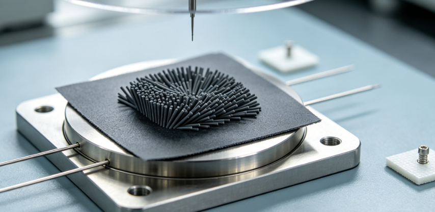
Precision Morphological and Dimensional Profiling by Advanced Electron Microscopy
The rod‑like morphology—diameter, length, aspect ratio, and straightness—directly influences quantum confinement, percolation behaviour, and mechanical reinforcement. We employ a combination of field‑emission scanning electron microscopy (FE‑SEM) and aberration‑corrected transmission electron microscopy (AC‑TEM) at accelerating voltages up to 300 kV. Using automated image analysis algorithms on >500 individual nanorods per batch, we report diameter distributions (mean, D10, D50, D90) with a precision of ±0.2 nm, length distributions (via SEM image stitching), and aspect ratio histograms with repeatability of < 1.5% RSD. For detailed lattice imaging, we use high‑resolution TEM (HRTEM) to resolve (111), (220), and (002) lattice fringes with sub‑ångström resolution (0.08 nm), and we perform selected area electron diffraction (SAED) and nanobeam diffraction to identify growth direction (e.g., [111] or [0001]) and to detect any amorphous shell or twinning defects. We also utilise scanning TEM (STEM) with high‑angle annular dark‑field (HAADF) imaging for Z‑contrast mapping, revealing surface contamination, oxide patches, or catalyst particles at the tips. For 3D morphological characterisation, we perform electron tomography (ET) with tilt series acquisition (‑70° to +70°, 2° increment) and reconstruct the volume‑specific surface area and internal pore accessibility with sub‑nanometre isotropic resolution.
Crystalline Polytype, Phase Purity, and Strain Analysis
The electronic and optical properties of SiC are strongly polytype‑dependent (cubic 3C‑SiC vs. hexagonal 4H‑ or 6H‑SiC), and the presence of even a few percent of secondary polytypes or free carbon can degrade device performance. We employ high‑resolution powder X‑ray diffraction (HR‑XRD) with synchrotron radiation (λ = 0.8–1.2 Å) or a state‑of‑the‑art laboratory diffractometer (Cu Kα, λ = 1.5406 Å), scanning over a 2θ range of 10–140° with a step size of 0.003°. Full Rietveld refinement is applied to quantify the relative fractions of 3C, 4H, and 6H polytypes with an accuracy of ±0.3 wt%, to determine lattice parameters (precision ±0.0002 Å), and to calculate crystallite size (via Scherrer and Williamson‑Hall methods) and microstrain. For nanorods with preferential orientation, we perform texture analysis (pole figures) to assess the degree of alignment. We complement XRD with Raman microspectroscopy (with 532 nm and 785 nm excitations), acquiring spectra over 100–2000 cm⁻¹. We analyse the characteristic peaks of SiC (TO and LO modes at ~790 and ~970 cm⁻¹ for 3C, and the folded modes for 4H/6H), and we quantify the intensity ratio of the D‑band (defect‑induced) to the G‑band (graphitic) for any free carbon, with a repeatability of < 2% for peak intensity ratios. Raman mapping (with step size of 200 nm) is used to generate spatial distribution maps of polytype homogeneity and defect density across individual nanorods.
Elemental Composition, Stoichiometry, and Ultra‑Trace Impurity Profiling
The Si/C molar ratio (stoichiometry) and the presence of metallic catalysts (e.g., Fe, Ni, Au) or unintentional dopants (N, Al, B) are critical to electrical and optical properties. We determine total silicon and carbon by combustion‑infrared detection (for C) and ICP‑OES after alkaline fusion (for Si), with relative expanded uncertainties (k=2) of < 0.5%. For ultra‑trace elements (catalyst residues, heavy metals, and rare earths), we digest the nanorods in a microwave‑assisted HF/HNO₃ system and analyse by inductively coupled plasma tandem mass spectrometry (ICP‑MS/MS) with collision/reaction cell (O₂, NH₃, H₂), achieving detection limits of 0.01–0.5 ppb for over 50 elements. We also quantify nitrogen and oxygen by inert gas fusion (IGF) with detection limits of 5 ppm. For surface‑sensitive composition, we use X‑ray photoelectron spectroscopy (XPS) with monochromatic Al Kα source and depth profiling (Ar⁺ cluster sputtering) to obtain Si 2p, C 1s, and O 1s core‑level spectra, distinguishing Si‑C, Si‑O, and C‑C/C‑O bonding states and quantifying the native oxide thickness (typically 0.5–2 nm) with precision of ±0.1 nm. The XPS data are further used to calculate the surface Si/C ratio and to detect any segregated impurities.
Surface Chemistry, Defect States, and Oxide Layer Characterisation
The surface of SiC nanorods is often covered by a thin silicon oxide layer and may host dangling bonds, carbon clusters, or adsorbed species that affect charge carrier dynamics and photocatalytic activity. In addition to XPS, we employ low‑energy electron energy loss spectroscopy (LEELS) in TEM to probe surface electronic states, and electron paramagnetic resonance (EPR) at X‑band (9.5 GHz) and Q‑band (34 GHz) at cryogenic temperatures (4–300 K) to identify paramagnetic defects (e.g., silicon vacancies, carbon vacancies, and dangling bonds) and to quantify their spin density (spins/g) with a sensitivity of 10⁹ spins/G. We also perform photoluminescence (PL) spectroscopy at room temperature and 77 K using a solid‑state laser (325 nm) and a spectrograph with CCD, recording the near‑band‑edge emission (around 380–420 nm for 3C‑SiC) and defect‑related deep‑level emissions (500–700 nm). The intensity ratio of band‑to‑band to defect emission (INBE/IDL) is used as a quality index for crystalline perfection, with repeatability of < 3%. We also perform time‑resolved PL (TRPL) with a picosecond pulsed laser to measure the carrier lifetime and to evaluate surface recombination velocity, which is critical for photodetector and solar cell applications.
Thermal Stability, Oxidation Resistance, and Phase Transformation Kinetics
High‑temperature stability is paramount for applications in harsh environments. We conduct simultaneous Thermogravimetric Analysis and differential scanning calorimetry (TGA‑DSC) from 30 °C to 1500 °C under synthetic air, argon, and reducing (5% H₂/N₂) atmospheres, at heating rates of 2, 5, and 10 °C/min. We determine the oxidation onset temperature (Ton) for the formation of SiO₂, the maximum oxidation rate (Tmax), and the total mass gain, with reproducibility of ±2 °C and ±0.1% mass. Coupled evolved gas analysis by mass spectrometry (EGA‑MS) identifies and quantifies CO, CO₂, and H₂O release, allowing us to distinguish between surface oxidation and bulk decomposition. We also perform isothermal oxidation experiments at 1000, 1200, and 1400 °C for up to 100 hours, followed by cross‑sectional TEM and XPS to measure the oxide scale thickness and composition, and to detect any carbon‑rich interfacial layers. The oxidation kinetics are modelled using parabolic (diffusion‑controlled) and linear (interface‑controlled) laws, and we calculate the apparent activation energy (Ea) via Arrhenius fitting. For phase transformation (e.g., 3C → 6H), we use in situ high‑temperature XRD up to 1400 °C to monitor changes in lattice parameters and polytype fractions in real time.
Dispersion, Surface Charge, and Colloidal Stability
For solution‑processing of nanorods into films or composites, dispersion stability is a key factor. We measure zeta potential as a function of pH (2–12) and ionic strength (0.001–1 M NaCl) using electrophoretic light scattering (ELS) with automatic titration, achieving precision of ±0.5 mV. We also perform dynamic light scattering (DLS) and nanoparticle tracking analysis (NTA) on diluted dispersions to obtain the hydrodynamic size distribution and polydispersity index (PdI) in various solvents (water, ethanol, NMP, etc.). We evaluate sedimentation stability using a multiple‑sample light scattering analyser (Turbiscan) over 24 hours, providing a stability index that predicts agglomeration behaviour in coating or casting formulations.
Our Distinctive Competencies and Analytical Superiority
Our service is uniquely distinguished by the orthogonal, fully cross‑validated integration of AC‑TEM (including tomography), synchrotron HR‑XRD, Raman mapping, ICP‑MS/MS, XPS, EPR, PL/TRPL, and TGA‑EGA‑MS—all performed on the same representative nanorod batch to eliminate sample‑to‑sample variability and to enable direct correlations (e.g., polytype vs. PL emission, impurity content vs. oxidation activation energy). We operate under ISO/IEC 17025 accreditation with dedicated glovebox facilities for oxygen‑sensitive handling. Our proprietary data fusion and predictive platform combines over 35 parameters (including diameter, polytype fraction, defect spin density, oxide thickness, Ton, and PL ratio) into a single “SiC Nanorod Performance Index” (SNPI™) that predicts field‑emission turn‑on field, photocatalytic hydrogen evolution rate, and high‑temperature composite strength. This index has been validated against >30 commercial and research‑grade SiC nanorod samples.
We achieve exceptional measurement precision: < 0.2 nm for diameter, < 0.3 wt% for polytype fraction, < 1.0% for Si/C ratio, < 0.5 nm for oxide thickness, and < 2% for oxidation onset temperature. Our turnaround time for the full characterisation suite (including high‑temperature oxidation and EPR) is 12–18 working days, with expedited 8‑day service for urgent material qualification. Crucially, our team of PhD‑level solid‑state physicists, inorganic chemists, and electron microscopists provides a comprehensive interpretative report that translates each measured parameter into actionable guidance—e.g., how to adjust growth temperature to minimise stacking faults, how to remove residual catalyst particles without damaging the oxide layer, or how to correlate the PL defect peak with surface passivation strategies. With over 20 successful projects on SiC nanowires and nanorods, we empower our clients to achieve synthesis reproducibility, eliminate performance‑limiting defects, and accelerate device development for optoelectronics, photocatalysis, and extreme‑environment sensors—all with the highest level of scientific rigour and technical credibility.