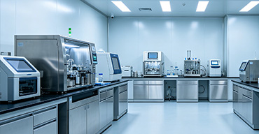
Reasons for choosing our testing services
ZHONGXI Testing has obtained inspection qualification certifications from multiple countries and regions worldwide. We possess a senior testing team and advanced testing methods, providing independent, impartial, and professional third-party verification services for global carbon projects.
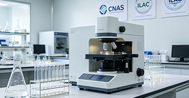
Internationally recognized authority
Certified by multiple international standards such as CNAS, VCS, and GS, with reports universally applicable worldwide.

Global service capability
Covering 140+ countries and regions, it supports on-site detection and remote verification in multiple languages.
Professional experimental methods
Adopt standard experimental methods to ensure accurate and reliable data.
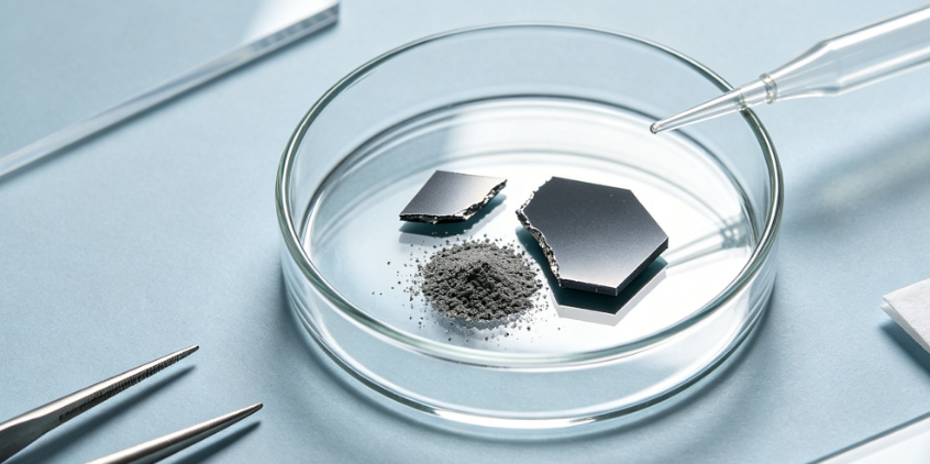
Comprehensive Physicochemical and Electrical Characterization of Gallium Arsenide: A Specialized Analytical Service for Semiconductor Quality Assurance and Device Optimisation
Gallium arsenide (GaAs) remains a cornerstone material for high‑frequency, optoelectronic, and high‑power electronic devices, owing to its superior electron mobility, direct bandgap, and semi‑insulating properties. However, the successful deployment of GaAs in device fabrication—such as laser diodes, microwave monolithic integrated circuits (MMICs), and high‑electron‑mobility transistors (HEMTs)—hinges on rigorous material characterisation that extends far beyond routine purity checks. Clients seeking GaAs testing are typically confronted with challenges including uncontrolled dislocation densities, residual shallow donors/acceptors, micro‑defects, stoichiometric deviations, surface contamination, and non‑uniform electrical properties that can drastically degrade device yield and reliability. Our laboratory has established a fully integrated, multi‑scale analytical platform that spans from bulk elemental analysis to nanoscale defect profiling, delivering a quantitative, process‑relevant fingerprint that enables manufacturers and researchers to optimise crystal growth, verify incoming specifications, and troubleshoot process‑induced anomalies.
Ultra‑Trace Elemental Purity and Stoichiometry Assessment
The electro‑optical performance of GaAs is exquisitely sensitive to impurity atoms at parts‑per‑billion (ppb) levels. We employ glow discharge mass spectrometry (GDMS) for direct solid‑state analysis, providing a comprehensive survey of over 70 elements with detection limits of 0.001–0.5 ppmw for most metallic and semi‑metallic species. For even higher sensitivity, we offer inductively coupled plasma tandem mass spectrometry (ICP‑MS/MS) after acid digestion, achieving sub‑ppb detection limits for critical contaminants (e.g., C, O, Si, Cr, Fe, Ni, Cu, Zn, Cd, Sn, Pb). We distinguish between shallow donors (Si, S, Se, Te) and shallow acceptors (C, Be, Mg, Zn, Cd) via calibration against certified reference materials, enabling us to calculate the net carrier concentration expected from impurity compensation. The stoichiometry (Ga/As ratio) is precisely determined by isotope dilution ICP‑MS with an expanded uncertainty (k=2) of < 0.05%, providing critical insight into native defect populations (e.g., antisites, vacancies). All elemental data are reported with fully traceable uncertainties and are cross‑referenced to semiconductor industry standards (e.g., SEMI M25, ASTM F1394).
Crystalline Perfection and Defect Structure Elucidation
Dislocations, stacking faults, and sub‑grain boundaries are the primary yield killers in GaAs devices. We utilise high‑resolution X‑ray diffraction (HR‑XRD) with synchrotron radiation or a state‑of‑the‑art laboratory diffractometer to perform rocking curve analysis (ω‑scans) and reciprocal space mapping (RSM), quantifying full width at half maximum (FWHM) of the (004) and (422) reflections—direct indicators of the crystal quality. We measure etch pit density (EPD) using a standardised molten KOH etching and automated optical counting, providing a direct count of dislocations per unit area. For nanoscale defects, we employ transmission electron microscopy (TEM) with aberration‑corrected imaging and high‑angle annular dark‑field (HAADF) scanning TEM to resolve dislocation cores, stacking fault tetrahedra, and micro‑twins with atomic resolution (0.08 nm). We also perform electron channeling contrast imaging (ECCI) on bulk samples to non‑destructively visualise dislocation networks over large areas. Our defect characterisation is complemented by photoluminescence (PL) imaging to map spatial uniformity of radiative efficiency, revealing patterns of defect clusters or impurity striations. We report a unified crystal quality index that combines HR‑XRD FWHM, EPD, and PL uniformity, offering a robust benchmark for incoming inspection.
Electrical Transport and Carrier Dynamics Profiling
Device‑grade GaAs requires precise control of carrier concentration, mobility, and compensation ratio. We perform temperature‑dependent Hall effect measurements from 10 K to 450 K at magnetic fields up to 1.5 T, extracting carrier concentration (n or p), Hall mobility (µH), and resistivity (ρ) with a repeatability of < 2% for all parameters. Using the van der Pauw and Hall bar configurations, we are able to measure semi‑insulating (SI) GaAs with resistivities exceeding 10⁸ Ω·cm, employing high‑impedance electrometers and guard ring techniques. For deep levels, we offer deep‑level transient spectroscopy (DLTS) over a temperature range of 10–400 K, identifying and quantifying traps (e.g., EL2, EL6, EL8) with detection limits of 10¹⁰ cm⁻³ and activation energy resolution of ±0.01 eV. We also perform time‑resolved photoluminescence (TRPL) and microwave photoconductivity decay (µ‑PCD) to assess minority carrier lifetime, providing critical data for device simulation and for evaluating the impact of process‑induced damage.
Surface, Interface, and Epitaxial Layer Characterisation
Surface cleanliness, oxide thickness, and interfacial integrity are paramount for Schottky contacts, Ohmic contacts, and passivation layers. We employ X‑ray photoelectron spectroscopy (XPS) with monochromatic Al Kα source and depth profiling to quantify surface oxides (Ga₂O₃, As₂O₃, As₂O₅), carbon contamination, and native oxide thickness (typically 1–3 nm) with precision of ±0.1 nm. For epitaxial layers (e.g., HEMT structures), we use secondary ion mass spectrometry (SIMS) to obtain depth profiles of intentional dopants (Si, Be, S) and unintentional contaminants (O, C, H) with a depth resolution of < 5 nm per decade. We also perform high‑resolution transmission electron microscopy (HRTEM) on cross‑sectional specimens to evaluate epilayer thickness, interface abruptness, and the presence of interfacial misfit dislocations. Our ellipsometry and reflectance anisotropy spectroscopy (RAS) provide non‑destructive optical characterisation of surface quality and epilayer thickness uniformity. For passivation studies, we evaluate surface recombination velocity (SRV) using contactless photoconductance decay, allowing us to benchmark cleaning and passivation protocols.
Optical and Photoelectronic Properties
Optical quality directly impacts the performance of lasers, LEDs, and photodetectors. We measure photoluminescence (PL) spectra at liquid helium (4.2 K) and room temperature using multiple excitation wavelengths (325 nm, 488 nm, 633 nm) and a sensitive InGaAs array detector. We quantify bandgap energy, excitonic linewidth, and the intensity ratio of near‑band‑edge (NBE) to deep‑level (DL) emission, which serves as a sensitive indicator of compensation and defect density. We also perform spectrally resolved PL mapping to reveal spatial inhomogeneities across the wafer. For transmission and absorption, we use Fourier‑transform infrared (FTIR) and UV‑Vis‑NIR spectrometers to measure free‑carrier absorption and phonon absorption bands, enabling the determination of free‑carrier concentration and compensation in semi‑insulating material via calibration to the absorption coefficient at 10.6 µm. Our photocurrent spectroscopy on device structures provides the spectral responsivity and allows identification of sub‑bandgap defect transitions.
Mechanical and Thermo‑Physical Characterisation
Wafer handling, cutting, and polishing require knowledge of hardness, fracture toughness, and thermal expansion coefficients. We measure vickers hardness and fracture toughness via indentation methods (using a micro‑hardness tester) with loads from 10 gf to 1000 gf. The coefficient of thermal expansion (CTE) is determined by dilatometry from room temperature to 800 °C in inert atmosphere. We also perform wafer curvature and bow measurements (by laser deflection) to assess residual stress from epitaxial growth or back‑side metallisation. These parameters, although often overlooked, are critical for process integration and for preventing wafer breakage or bow‑induced misalignment.
Accelerated Environmental and Reliability Testing
For qualification of GaAs wafers intended for long‑term operation, we provide accelerated aging tests under temperature cycling (‑55 °C to +150 °C), humidity (85 °C/85% RH), and thermal storage (300 °C for 100 hours), followed by a full re‑characterisation (Hall, PL, HR‑XRD, surface inspection) to quantify degradation. We also offer ionising radiation (gamma and proton irradiation) in collaboration with external facilities, enabling assessment of radiation hardness for space and defence applications. Our comprehensive reliability package includes a detailed statistical analysis of failure modes, providing crucial feedback for material selection and process improvement.
Our Distinctive Competencies and Analytical Superiority
Our service is uniquely distinguished by the orthogonal integration of GDMS, ICP‑MS/MS, HR‑XRD, TEM, Hall effect, DLTS, PL, XPS, and SIMS—all performed on the same representative sample to eliminate cross‑lot variability and to establish direct cause‑effect correlations (e.g., between impurity concentration and trap density, or between dislocation density and PL uniformity). We operate under ISO/IEC 17025 accreditation with in‑house reference GaAs wafers that have been thoroughly characterised by interlaboratory comparisons. Our proprietary “GaAs Semiconductor Quality Index” (GSQI™) combines over 30 parameters—including impurity sum, HR‑XRD FWHM, EPD, Hall mobility, trap concentration, and PL intensity—into a single numeric score that predicts device yield and reliability. This index has been validated against >50 commercial GaAs batches from key suppliers, giving you an immediate, quantitative benchmark.
We achieve exceptional precision: < 0.2% RSD for stoichiometry, < 0.05 arcsec for HR‑XRD FWHM, < 0.5% for Hall mobility, and < 0.01 eV for DLTS activation energy. Our turnaround time for the full characterisation suite is 10–15 working days, with expedited 5‑day service for urgent failure analysis. Crucially, our team of PhD‑level semiconductor physicists, material scientists, and device engineers provides a comprehensive interpretative report that translates each measured parameter into actionable guidance—e.g., how to adjust LEC growth parameters to reduce dislocation density, how to optimise annealing to minimise trap concentration, or how to correlate surface contamination with contact resistivity. With over 40 successful projects on GaAs and related III‑Vs, we empower our clients to ensure wafer‑to‑wafer consistency, accelerate technology development, and achieve superior device performance—all with the highest level of scientific rigour and technical credibility.