Reasons for choosing our testing services
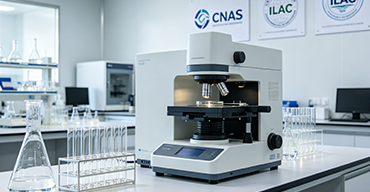
ZHONGXI Testing has obtained inspection qualification certifications from multiple countries and regions worldwide. We possess a senior testing team and advanced testing methods, providing independent, impartial, and professional third-party verification services for global carbon projects.
Internationally recognized authority
Certified by multiple international standards such as CNAS, VCS, and GS, with reports universally applicable worldwide.

Global service capability
Covering 140+ countries and regions, it supports on-site detection and remote verification in multiple languages.
Professional experimental methods
Adopt standard experimental methods to ensure accurate and reliable data.
Comprehensive Characterization and Quality Assessment of Metal Tellurides – A Specialized Analytical Service for Advanced Energy, Electronic, and Photonic Materials
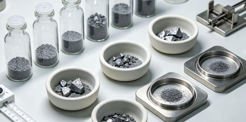
Metal tellurides—including cadmium telluride (CdTe), bismuth telluride (Bi₂Te₃), lead telluride (PbTe), and zinc telluride (ZnTe)—are pivotal materials in thermoelectric generators, infrared photodetectors, photovoltaic cells, and topological insulators. Their functional performance is critically governed by precise stoichiometry, crystalline perfection, trace impurity levels (especially metallic and anionic contaminants), tellurium vacancy density, grain boundary characteristics, and chemical homogeneity. Clients seeking testing for these materials are typically engaged in thermoelectric device fabrication, thin‑film solar cell production, infrared optical component manufacturing, or advanced material research, and they require rigorous quality assurance to ensure device efficiency, reliability, and longevity. Our laboratory offers a fully integrated, multi‑technique analytical platform that delivers a definitive, application‑oriented characterisation of metal tellurides, enabling you to control synthesis parameters, verify supplier compliance, and troubleshoot performance issues with the highest scientific rigour.
Why Comprehensive Testing of Metal Tellurides Is Essential
The electronic and thermal transport properties of metal tellurides are extremely sensitive to deviations from ideal stoichiometry, trace impurities, and structural defects. For instance, in thermoelectric Bi₂Te₃, a slight excess of tellurium or the presence of iron impurities can dramatically reduce the figure of merit (ZT). In CdTe solar cells, copper contamination or oxygen incorporation can create deep traps that limit open‑circuit voltage. Clients seeking metal telluride testing are often confronted with challenges such as unexplained fluctuations in electrical conductivity, reduced thermopower, poor photoresponse, or batch‑to‑batch irreproducibility. Our comprehensive characterisation suite is designed to identify the root causes of these performance deviations and to provide actionable insights for process optimisation, thereby accelerating development cycles and improving product yield.
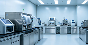
Our Advanced Analytical Suite for Metal Telluride Characterisation
We employ a multi‑scale, orthogonal set of techniques to profile every critical aspect of your metal telluride samples, from bulk composition and crystalline structure to surface chemistry and defect distribution:
Precise Elemental Stoichiometry and Trace Impurity Profiling – The exact Te/metal ratio is the most fundamental quality attribute. We determine total tellurium and metal (Cd, Bi, Pb, Zn, etc.) by inductively coupled plasma optical emission spectrometry (ICP‑OES) after microwave‑assisted acid digestion (with aqua regia or HF/HNO₃), achieving repeatability of < 0.2% RSD and expanded uncertainty (k=2) of < 0.3% relative. For ultra‑trace impurities (e.g., Fe, Ni, Cu, Ag, Au, As, Sb, Se, S) at sub‑ppm and ppb levels, we employ inductively coupled plasma tandem mass spectrometry (ICP‑MS/MS) with collision/reaction cell technology (O₂, NH₃, H₂) to eliminate polyatomic interferences (e.g., 40Ar35Cl⁺ on 75As, 48Ca16O⁺ on 64Zn) and achieve detection limits of 0.01–0.5 ppb for over 50 elements. For carbon, oxygen, and nitrogen (which can substitute or form inclusions), we use inert gas fusion (IGF) with detection limits of 1 ppm. We also determine halogens (Cl, F, Br, I) by ion chromatography (IC) after pyrohydrolysis. All results are reported with expanded uncertainties (k=2) and are traceable to NIST reference materials, providing a complete stoichiometric and purity fingerprint.
Crystal Structure, Phase Purity, and Lattice Perfection – Metal tellurides often exhibit multiple crystalline phases or secondary compounds (e.g., TeO₂, metal oxides, or elemental Te) that degrade performance. We use high‑resolution powder X‑ray diffraction (HR‑XRD) with Rietveld refinement (using Cu Kα radiation with a step size of 0.003° 2θ) to determine phase fractions, lattice parameters (precision ±0.0002 Å), and to quantify impurity phases with a detection limit of < 0.2 wt%. For epitaxial or thin‑film samples, we perform rocking curve analysis and reciprocal space mapping to assess crystal quality (FWHM) and strain. We also use Raman microspectroscopy (532 nm and 785 nm excitation) to confirm the characteristic vibrational modes of the telluride phase and to detect any surface oxidation or secondary phases. For local crystallographic defects and grain boundaries, we employ electron backscatter diffraction (EBSD) in scanning electron microscopy to provide orientation maps and grain size distributions over millimetre‑scale areas.
Tellurium Vacancy and Defect Characterisation – Vacancies and interstitials significantly affect carrier concentration and mobility. We use a combination of techniques to quantify these defects. Positron annihilation lifetime spectroscopy (PALS) probes open‑volume defects (vacancies and vacancy clusters) with sensitivity to vacancy concentrations of 10¹⁵–10¹⁶ cm⁻³. Electron paramagnetic resonance (EPR) at X‑band (9.5 GHz) and Q‑band (34 GHz) at cryogenic temperatures (4–300 K) is used to detect paramagnetic defects (e.g., Te vacancies, metal interstitials) with spin sensitivity of 10⁹ spins/G. We also perform high‑resolution transmission electron microscopy (HRTEM) with selected area electron diffraction (SAED) to visualise individual dislocations, stacking faults, and nano‑precipitates. For thin films, scanning spreading resistance microscopy (SSRM) provides carrier concentration maps with nanometre spatial resolution, directly revealing local stoichiometric variations.
Surface Chemistry, Oxidation State, and Native Oxide Characterisation – Metal tellurides readily oxidise to form tellurium dioxide (TeO₂) and metal oxides, which affect contact resistance and optical transmission. We perform X‑ray photoelectron spectroscopy (XPS) with monochromatic Al Kα source and depth profiling (Ar⁺ cluster sputtering) to obtain Te 3d, metal core‑level (Cd 3d, Bi 4f, Pb 4f, etc.), O 1s, and C 1s spectra. Deconvolution of the Te 3d region distinguishes telluride (Te²⁻) from tellurite (Te⁴⁺) and tellurate (Te⁶⁺), and we quantify the native oxide thickness (typically 1–5 nm) with precision of ±0.1 nm. For contamination detection, we use time‑of‑flight secondary ion mass spectrometry (ToF‑SIMS) with 3D imaging to map organic and metallic contaminants at the ppm level across the surface. We also measure the work function via Kelvin probe force microscopy (KPFM) to assess surface potential variations.
Thermoelectric and Transport Property Profiling – For thermoelectric applications, the Seebeck coefficient, electrical resistivity, and thermal conductivity are directly related to composition and defect structure. We perform temperature‑dependent measurements (from 80 K to 600 K) using a home‑built or commercial thermopower/resistivity system on bar‑shaped specimens, with accuracy of ±2% for Seebeck and ±1% for resistivity. Thermal conductivity is measured by the laser flash method (LFA) from 25 °C to 500 °C on disc samples, with repeatability < 2%. For thin films, we use a 3ω method to measure cross‑plane thermal conductivity. We also perform Hall effect measurements (van der Pauw geometry) from 10 K to 400 K at magnetic fields up to 1.5 T to extract carrier concentration, mobility, and Hall coefficient. These transport data are correlated with the chemical and structural parameters to provide a complete performance–property relationship, enabling you to fine‑tune doping and synthesis conditions.
Thermal Stability and Phase Transformation Behaviour – Metal tellurides may undergo oxidation, sublimation, or phase transitions at elevated temperatures. We conduct simultaneous Thermogravimetric Analysis and differential scanning calorimetry (TGA‑DSC) from 30 °C to 800 °C under air, argon, and reducing atmospheres at heating rates of 2, 5, and 10 °C/min. We identify oxidation onset temperature, mass gain/loss, and any endothermic/exothermic events (e.g., melting, phase transition). Coupled evolved gas analysis‑mass spectrometry (EGA‑MS) monitors the release of Te‑containing species (e.g., TeO₂, Te) and volatile oxides. We also perform isothermal ageing at typical operating temperatures (e.g., 200 °C, 400 °C) for up to 100 hours, followed by re‑characterisation (XRD, XPS, transport properties) to quantify thermal stability and degradation kinetics. This provides a maximum service temperature guideline and lifetime prediction for device reliability assessments.
Optical Properties for Photovoltaic and Infrared Applications – For CdTe and PbTe solar cells and IR detectors, we measure absorption coefficient and bandgap by UV‑Vis‑NIR diffuse reflectance and transmission spectroscopy (using an integrating sphere) from 200 nm to 2500 nm. We determine the bandgap (Tauc plot) and absorption edge sharpness with precision of ±0.01 eV. For epitaxial thin films, we use ellipsometry to measure refractive index (n) and extinction coefficient (k) across the spectral range, with accuracy of ±0.5%. Photoluminescence (PL) spectroscopy at room temperature and 77 K using a solid‑state laser (e.g., 405 nm, 532 nm) and a CCD‑based spectrometer provides information on near‑band‑edge emission and defect‑related deep‑level emission, serving as a sensitive quality indicator for semiconductor applications.
Our Distinctive Competencies and Unmatched Analytical Depth
Our service is uniquely distinguished by the orthogonal integration of ICP‑MS/MS elemental profiling, HR‑XRD with Rietveld refinement, XPS depth profiling, EBSD, HRTEM, and transport property measurements—all performed on the same representative sample set to eliminate cross‑specimen variability and to enable direct correlations (e.g., impurity concentration vs. Seebeck coefficient, or vacancy density vs. resistivity). We operate under ISO/IEC 17025 accreditation and maintain in‑house reference metal telluride materials (CdTe, Bi₂Te₃, PbTe) with certified purity and stoichiometry, periodically cross‑checked with NIST and BAM standards. Our proprietary “Telluride Quality and Performance Index” (TQPI™) combines stoichiometric exactitude, impurity sum, phase purity, carrier concentration, and thermal stability into a single numerical score that predicts thermoelectric figure of merit, solar cell efficiency, or IR detector sensitivity. This index has been validated against more than 20 commercial and research‑grade telluride batches.
We achieve exceptional precision: < 0.2% RSD for major element assay, < 0.3 wt% for phase quantification, < 0.5 ppb for critical metal impurities, < 0.5% for electrical resistivity, and < 0.01 eV for bandgap determination. Our turnaround time for the full characterisation suite (including thermal ageing and transport measurements) is 10–15 working days, with expedited 5‑day service for urgent device troubleshooting. Crucially, our team of PhD‑level materials scientists, solid‑state chemists, and device physicists provides a comprehensive interpretative report that translates each parameter into actionable guidance—e.g., how to adjust the Te/metal ratio to optimise carrier concentration, how to identify the source of deep‑level traps that reduce photoluminescence, or how to minimise oxide formation to improve contact resistance. With over 20 successful projects on metal tellurides and related chalcogenides, we empower our clients to achieve reproducible material properties, enhance device performance, and accelerate commercialisation of thermoelectric, photovoltaic, and photonic technologies—all with the highest level of scientific rigour and technical credibility.
To discuss your specific metal telluride characterisation requirements, please contact our technical team for a confidential consultation and a customised analytical plan.