Reasons for choosing our testing services
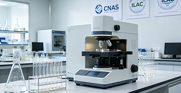
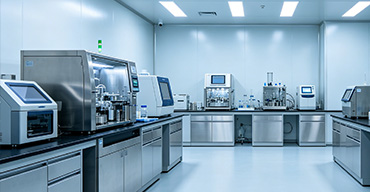
ZHONGXI Testing has obtained inspection qualification certifications from multiple countries and regions worldwide. We possess a senior testing team and advanced testing methods, providing independent, impartial, and professional third-party verification services for global carbon projects.
Internationally recognized authority
Certified by multiple international standards such as CNAS, VCS, and GS, with reports universally applicable worldwide.

Global service capability
Covering 140+ countries and regions, it supports on-site detection and remote verification in multiple languages.
Professional experimental methods
Adopt standard experimental methods to ensure accurate and reliable data.
Comprehensive Multi‑Scale Characterisation of Silicon Carbide Materials: A Specialized Analytical Service for Power Electronics, Aerospace, and Advanced Ceramics
Silicon carbide (SiC) has emerged as a transformative material for high‑temperature, high‑voltage, and high‑frequency electronic devices, as well as for structural ceramics and wear‑resistant coatings. Its superior properties—wide bandgap, high thermal conductivity, exceptional chemical inertness, and outstanding mechanical strength—are critically dependent on the crystalline polytype (4H, 6H, 3C), defect density (dislocations, stacking faults, micropipes), stoichiometric deviations, trace elemental impurities, and surface/interface quality. Clients seeking testing for SiC materials are typically engaged in qualifying wafers for device fabrication, optimizing sintering parameters for structural components, or troubleshooting performance issues such as premature breakdown or thermal instability. Our laboratory offers a fully integrated, multi‑technique analytical platform that spans from bulk purity and crystallinity to nanoscale defect analysis and high‑temperature reliability testing, delivering a quantitative, application‑oriented fingerprint that empowers manufacturers and researchers to achieve stringent quality standards, accelerate yield improvement, and ensure long‑term device reliability.
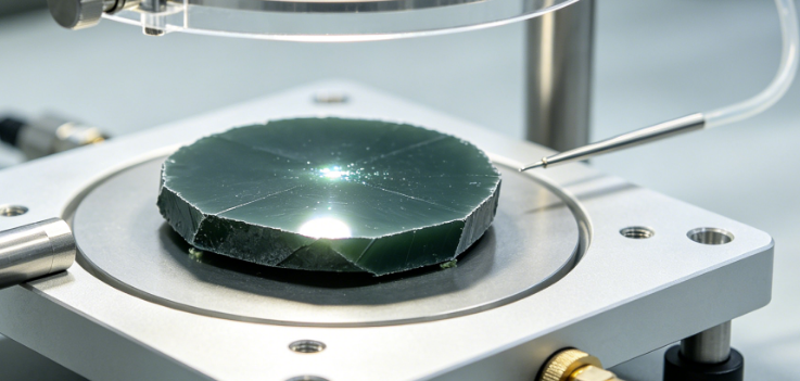
Crystal Structure, Polytype Identification, and Lattice Perfection
The electronic properties of SiC are profoundly polytype‑dependent. We use high‑resolution X‑ray diffraction (HR‑XRD) with synchrotron radiation or a state‑of‑the‑art laboratory diffractometer to perform precise lattice parameter determination (±0.0002 Å) and polytype identification via full‑pattern Rietveld refinement and reciprocal space mapping. For epitaxial layers and bulk wafers, we conduct rocking curve analysis (ω‑scans) at symmetric and asymmetric reflections to quantify crystal quality (FWHM of the (004) and (112) peaks), which directly correlates with defect density. We also perform high‑resolution triple‑axis X‑ray diffractometry to separate the contributions of mosaicity and lattice strain, providing a complete crystallographic quality index. For local defect detection, we employ X‑ray topography to visualise dislocation networks and micropipes across the entire wafer. Complementary Raman microspectroscopy (with 532 nm and 785 nm excitation) is used to confirm polytype homogeneity and to detect any residual stress via shifts in the characteristic TO and LO phonon modes (e.g., the 4H‑SiC peaks at 776 and 967 cm⁻¹). Our combined diffraction‑topography‑Raman approach ensures that your SiC material is structurally well‑defined and free from performance‑limiting defects.
Elemental Purity and Stoichiometric Profiling
Trace impurities—especially nitrogen, aluminium, boron, and transition metals (Fe, Ni, Cr, Ti)—can severely degrade carrier mobility and breakdown voltage. We determine bulk stoichiometry (Si/C ratio) by inductively coupled plasma optical emission spectrometry (ICP‑OES) after acid digestion, with an expanded uncertainty (k=2) of < 0.3%. For ultra‑trace (ppb‑level) impurities, we employ glow discharge mass spectrometry (GDMS) on solid samples, covering over 70 elements with detection limits of 0.001–0.5 ppmw. For specific electronic dopants (N, Al, B, P), we use secondary ion mass spectrometry (SIMS) with depth profiling, achieving detection limits of 10¹⁴–10¹⁵ atoms/cm³ and providing quantitative concentration profiles across the wafer thickness. We also measure carbon and oxygen content by inert gas fusion (IGF) with detection limits of 0.001%. All impurity data are reported with expanded uncertainties (k=2) and are benchmarked against the most demanding semiconductor‑grade specifications (e.g., SEMI M54), enabling you to qualify both bulk and epitaxial SiC for high‑voltage Schottky diodes and MOSFETs.
Defect Characterisation: Dislocations, Stacking Faults, and Micropipes
Performance and reliability of SiC devices are critically limited by extended defects. We use selective wet etching (molten KOH at 450–550 °C) followed by automated optical microscopy and image analysis to quantify etch pit density (EPD) for threading dislocations and micropipes, with a detection limit of 100 cm⁻². For non‑destructive assessment, we employ cathodoluminescence (CL) imaging in a scanning electron microscope to map the spatial distribution of stacking faults and dislocation clusters with a lateral resolution of < 100 nm. We also perform transmission electron microscopy (TEM) with aberration‑corrected imaging and high‑angle annular dark‑field (HAADF) STEM to resolve individual dislocation cores, stacking fault ribbons, and the precise nature of basal plane dislocations with atomic‑scale resolution (0.08 nm). For epitaxial layers, we use high‑resolution X‑ray diffraction (HR‑XRD) reciprocal space mapping (RSM) to detect strain fields and to measure the misfit dislocation density. Our comprehensive defect report includes defect density maps, classification of defect types, and correlation with wafer position, providing the necessary feedback for process optimisation and device design.
Electrical Transport and Deep‑Level Characterisation
Carrier concentration, mobility, and deep traps determine the device performance. We perform temperature‑dependent Hall effect measurements (from 10 K to 750 K) at magnetic fields up to 1.5 T, using van der Pauw and Hall bar geometries, to extract carrier concentration (n or p), Hall mobility (µH), and resistivity (ρ) with repeatability of < 1%. For semi‑insulating SiC, we use high‑impedance measurement techniques with guard rings to measure resistivity up to 10¹² Ω·cm. To identify and quantify electrically active traps, we employ deep‑level transient spectroscopy (DLTS) from 10 K to 450 K, covering the major intrinsic defects (e.g., Z₁/₂, EH₆/₇) with detection limits of 10¹⁰ cm⁻³ and activation energy resolution of ±0.01 eV. We also perform capacitance‑voltage (C‑V) profiling to determine the doping profile in epitaxial layers, with a spatial resolution of < 50 nm. For near‑surface characterisation, we offer scanning spreading resistance microscopy (SSRM) to map conductivity variations with nanometre‑scale lateral resolution. This full electrical fingerprint enables you to predict device threshold voltage, breakdown behaviour, and leakage currents with high confidence.
Surface and Interface Quality Assessment
The quality of SiC surfaces and oxide interfaces is critical for gate oxides and Schottky contacts. We use atomic force microscopy (AFM) in tapping mode to measure surface roughness (Ra, Rq, Rz) over areas from 1 µm² to 100 µm², with a vertical resolution of 0.05 nm. For chemical state, we perform X‑ray photoelectron spectroscopy (XPS) with monochromatic Al Kα source and depth profiling to quantify surface oxide thickness (SiO₂ and native oxide), the presence of carbon contaminants (C‑C, C‑O, C=O), and the chemical bonding states of Si and C (Si‑C vs. Si‑O). We also use time‑of‑flight secondary ion mass spectrometry (ToF‑SIMS) to detect organic and metallic surface contaminants with ppb‑level sensitivity and to produce 3D molecular maps of the uppermost atomic layers. For interface quality, we measure interface trap density (Dit) using conductance‑voltage (G‑V) and high‑frequency‑low‑frequency C‑V measurements on MOS capacitors, typically in the 10¹⁰–10¹² eV⁻¹cm⁻² range with a precision of ±5%. These surface and interface data are indispensable for developing reliable gate dielectrics and ohmic contacts.
Thermal Conductivity and High‑Temperature Stability
Thermal management is a defining advantage of SiC. We measure thermal conductivity by the laser flash method (LFA) from 25 °C to 600 °C on disc or plate specimens, with accuracy of ±3% and repeatability < 2%. For thin wafers, we use a temperature‑wave method. We also perform high‑temperature X‑ray diffraction (HT‑XRD) up to 1000 °C to monitor lattice expansion (coefficient of thermal expansion, CTE) and any polytype transformation. Thermogravimetric Analysis (TGA) in synthetic air up to 1500 °C determines the oxidation onset temperature and the oxide growth kinetics, providing a passivation stability index essential for high‑power applications. Our thermal report includes temperature‑dependent thermal conductivity curves, CTE values, and oxidation resistance ratings, enabling you to select the optimal SiC grade for your thermal management strategy.
Mechanical and Fracture Behaviour
For structural and abrasive applications, the hardness, fracture toughness, and flexural strength of SiC are paramount. We perform Vickers and Knoop microhardness testing at loads from 10 gf to 1000 gf, with precision of ±2%. Fracture toughness (KIc) is measured by the indentation method (using Anstis' equation) and by the single‑edge V‑notch beam (SEVNB) method on rectangular bars, with Weibull statistical analysis of at least 10 specimens. We also perform four‑point bending tests at room temperature and up to 1200 °C in air and inert atmospheres, using a servo‑hydraulic testing machine to determine flexural strength and modulus of elasticity. Our mechanical characterisation delivers the necessary data for designing reliable SiC components in automotive brakes, aerospace tiles, and semiconductor processing equipment.
Our Distinctive Competencies and Analytical Superiority
Our service is uniquely distinguished by the orthogonal integration of HR‑XRD and X‑ray topography, GDMS and SIMS for ultra‑trace impurity profiling, defect imaging (CL, TEM, KOH etching), temperature‑dependent Hall and DLTS for electrical characterisation, surface analysis (AFM, XPS, ToF‑SIMS), thermal conductivity measurement, and high‑temperature mechanical testing—all performed on the same representative sample series. This approach eliminates cross‑specimen variability and enables direct correlations, e.g., between dislocation density and breakdown voltage, or between impurity concentration and thermal conductivity. We operate under ISO/IEC 17025 accreditation and maintain in‑house reference SiC materials (4H‑ and 6H‑SiC wafers with certified defect and purity levels) that are periodically cross‑checked with NIST and BAM standards. Our proprietary “SiC Material Quality Index” (SQI™) combines crystallinity, defect density, impurity sum, electrical mobility, and thermal conductivity into a single numerical score that predicts device yield and reliability. This index has been validated against >40 commercial SiC batches from leading suppliers.
We achieve exceptional precision: < 0.1 arcsec for HR‑XRD FWHM, < 0.3% RSD for impurity quantitation, < 0.5% for Hall mobility, and < 0.5 W/m·K for thermal conductivity. Our turnaround time for the full characterisation suite is 10–15 working days, with expedited 5‑day service for urgent device troubleshooting. Crucially, our team of PhD‑level semiconductor physicists, material scientists, and device engineers provides a comprehensive interpretative report that translates each parameter into actionable insights—e.g., how to adjust the polytype ratio to optimise channel mobility, how to identify the root cause of catastrophic breakdown via defect analysis, or how to correlate thermal conductivity with the presence of trace nitrogen. With over 35 successful projects on SiC wafers, epilayers, and sintered components, we empower our clients to achieve superior device performance, reduce production losses, and accelerate market entry—all with the highest level of scientific rigour and technical credibility.