Reasons for choosing our testing services
ZHONGXI Testing has obtained inspection qualification certifications from multiple countries and regions worldwide. We possess a senior testing team and advanced testing methods, providing independent, impartial, and professional third-party verification services for global carbon projects.
Internationally recognized authority
Certified by multiple international standards such as CNAS, VCS, and GS, with reports universally applicable worldwide.

Global service capability
Covering 140+ countries and regions, it supports on-site detection and remote verification in multiple languages.
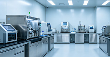
Professional experimental methods
Adopt standard experimental methods to ensure accurate and reliable data.
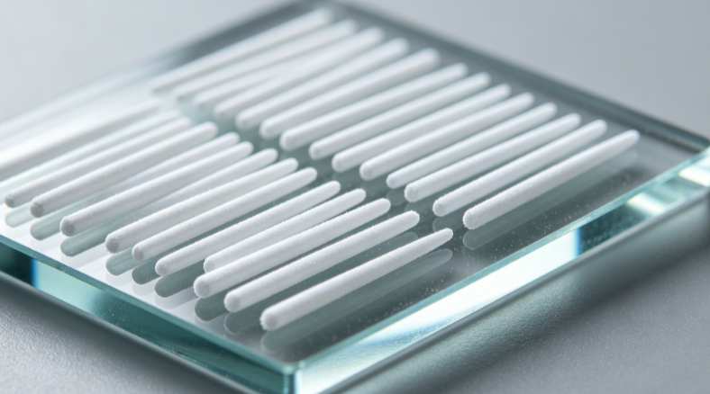
Zinc Oxide Nanorod Characterization – Complete Morphological, Structural, and Optical Analysis
If you are searching for zinc oxide (ZnO) nanorod testing, you are likely preparing to evaluate the quality, dimensions, crystal structure, or functional properties of your synthesized nanorods – whether for optoelectronics, gas sensors, photocatalysis, or biomedical applications. Our service provides a comprehensive, multi‑technique characterization platform that resolves nanorod length, diameter, aspect ratio, crystallographic orientation, surface chemistry, and defect‑related optical properties with sub‑nanometer precision. We deliver the data you need to correlate synthesis parameters with performance, ensuring batch‑to‑batch reproducibility and publication‑ready results.
What We Determine – From Individual Nanorods to Ensemble Properties
ZnO nanorods exhibit unique size‑, shape‑, and defect‑dependent behaviors. Our integrated analytical suite covers morphology, crystal structure, chemical state, light emission, and surface area using a combination of electron microscopy, X‑ray diffraction, spectroscopy, and porosimetry. Key measurable parameters include:
1. Morphology – length, diameter, aspect ratio, orientation – We employ high‑resolution scanning electron microscopy (HR‑SEM) at accelerating voltages down to 1 kV to image uncoated nanorods with 1.5 nm resolution. Automated image analysis (ImageJ with custom macro) measures length (20 nm to 10 µm) and diameter (5 nm to 500 nm) from at least 500 individual rods, providing statistically robust distributions (mean, median, standard deviation, D10/D50/D90). For vertical arrays, we measure alignment angle relative to substrate normal. Transmission electron microscopy (TEM) at 200 kV gives atomic‑scale lattice imaging (0.19 nm point resolution) to confirm single‑crystal vs polycrystalline nature and identify growth direction (e.g., [0001] along c‑axis).
2. Crystalline phase & texture – Powder X‑ray diffraction (XRD) with Cu Kα radiation and parallel beam optics identifies wurtzite ZnO (ICDD 00‑036‑1451) and detects secondary phases (e.g., Zn(OH)₂, ZnO₂) down to 1 wt%. We refine lattice parameters a and c to ±0.0005 Å and, for oriented nanorod films, measure pole figures to quantify (002) texture fraction. Crystallite size along c‑axis is calculated via Scherrer equation from (002) peak broadening, cross‑validated with TEM.
3. Surface chemistry & defect states – X‑ray photoelectron spectroscopy (XPS) surveys Zn 2p, O 1s, and C 1s, quantifying Zn/O atomic ratio (stoichiometry deviation), hydroxyl groups (O 1s peak at ~531.5 eV), and adventitious carbon. Detection limit 0.1 at%. For oxygen vacancies and zinc interstitials – key for photoluminescence – we use room‑temperature and low‑temperature (10 K) photoluminescence (PL) with a 325 nm HeCd laser. We deconvolute near‑band‑edge emission (NBE, ~380 nm) from deep‑level emission (DLE, 450‑700 nm) and report the NBE/DLE ratio as a defect density proxy. Spatial mapping of defects is possible via cathodoluminescence (CL) in SEM with 10 nm resolution.
4. Specific surface area & porosity – N₂ physisorption (BET) measures specific surface area from 0.5 to 200 m²/g (repeatability ±2%). For nanorod powders, we also report Barrett‑Joyner‑Halenda (BJH) pore size distribution (2‑200 nm) from the desorption branch, revealing inter‑rod mesoporosity.
5. Elemental purity & dopant quantification – ICP‑MS after microwave digestion quantifies major (Zn) and trace elements (Al, Ga, In, Mg, Fe, Cu, Cd, Pb) down to 0.01 ppm. For doped ZnO nanorods (e.g., Al‑ZnO), we provide dopant concentration in at% or wt% with ±2% relative accuracy.
Technical Performance Overview – Detection Limits & Resolutions
The table below summarizes our key analytical capabilities for ZnO nanorod characterization.
| Property / Parameter | Method(s) Used | Detection Range / Resolution | Typical Application Insight |
|---|---|---|---|
| Nanorod length & diameter
|
HR‑SEM + automated image analysis
|
Length: 20 nm – 10 µm (±2 nm); Diameter: 5 – 500 nm (±1 nm)
|
Batch uniformity, aspect ratio control for piezoelectric or sensing performance
|
| Crystallographic growth direction | Selected area electron diffraction (SAED) in TEM
|
Indexing to 0.1 nm⁻¹; orientation confirmed at atomic scale
|
Verify [0001] growth (c‑axis) or non‑polar direction; correlate with synthesis method
|
| Lattice parameters (a, c) | High‑resolution XRD, Rietveld refinement
|
a: ±0.0005 Å; c: ±0.0005 Å
|
Detect residual strain (peak shifts) or doping‑induced lattice expansion
|
| Oxygen vacancy / defect density | XPS (O 1s), PL (NBE/DLE ratio), EPR
|
XPS: 0.1 at% change in O‑deficient species; PL ratio ±0.05
|
Correlate defect concentration with photocatalytic activity or quenching of UV emission
|
| Surface area & porosity | BET (N₂ physisorption), BJH pore analysis
|
BET: 0.5‑200 m²/g ±2%; pore size 2‑200 nm
|
Assess agglomeration; predict adsorption capacity for gas sensors or dye removal
|
| Elemental composition (Zn, dopants, impurities) | ICP‑MS, EDS (SEM/TEM)
|
ICP‑MS: 0.01 ppm – wt%; EDS: 0.1 wt% (semi‑quantitative)
|
Quantify intentional doping (e.g., 2% Al) and detect unwanted contaminants
|
| Photoluminescence quantum yield (PLQY) | Absolute PL quantum yield measurement (integrating sphere)
|
0.1 – 100% ±1% absolute
|
Evaluate emission efficiency for LED or lasing applications
|
All results include measurement uncertainty (expanded, k=2) and are reported with full instrument conditions and raw data available upon request.
Why Choose Our ZnO Nanorod Testing Service?
Characterizing ZnO nanorods demands not only advanced instrumentation but also deep experience in interpreting nanoscale data – especially regarding defects and orientation. Our service offers distinct, practical advantages:
1. Complete correlative workflow from individual rods to bulk – We do not provide isolated numbers. Our report integrates HR‑SEM statistics, TEM lattice images, XRD texture analysis, and ensemble PL/XPS into a unified material card. You will see, for example, how the measured aspect ratio (from SEM) correlates with the crystallite size from XRD and how surface oxygen vacancies (XPS) explain the broad deep‑level emission (PL).
2. Nanoscale precision with automated statistics – Manual measurement of nanorods is biased and time‑consuming. We use machine‑learning‑assisted image segmentation (trained on >10,000 ZnO rods) to extract length/diameter distributions from SEM images. The software rejects overlapping or misoriented rods and provides histograms with kernel density fits – giving you true population statistics, not just “representative” images.
3. Deep defect analysis for functional tuning – ZnO nanorod performance (e.g., UV sensing, photocatalytic degradation) is dominated by intrinsic defects (VO, Zni). Our combined XPS‑PL‑EPR approach quantifies relative defect concentrations and distinguishes surface vs. bulk defects via angle‑resolved XPS and variable‑excitation‑wavelength PL. We provide a defect‑property correlation matrix that helps you adjust synthesis (annealing atmosphere, temperature) to achieve desired defect chemistry.
4. Ultra‑low sample consumption & flexible forms – We require only 1‑2 mg of powder or a 1 cm × 1 cm substrate with grown nanorods. We also accept dispersions (in water, ethanol) – we will deposit them onto grids for TEM/SEM. For research‑scale batches, this preserves your precious material while delivering full data.
5. Rapid turnaround for iterative R&D – Standard full characterization (SEM + TEM + XRD + XPS + PL + BET) for up to 8 samples is completed in 10‑12 business days. For fast iteration of synthesis parameters, we offer a “quick look” service (SEM + XRD + PL) within 48 hours on up to 3 samples.
6. Expertise in oriented arrays and single rods – We have extensive experience with vertically aligned ZnO nanorods grown by hydrothermal or electrochemical methods. We can measure rod alignment distribution (angle deviation from normal), areal density (rods/µm²), and for isolated rods, single‑rod TEM diffraction to confirm polar growth direction. This is critical for piezo‑nanogenerator and biosensor applications.
7. Environmental stability assessment – ZnO nanorods can degrade or hydrate in humid air. We offer accelerated aging studies (40°C/80% RH for up to 4 weeks) with periodic XRD and XPS to monitor formation of Zn(OH)₂ or ZnCO₃ surface layers. You receive a stability report with recommended storage conditions.
8. Publication‑ready reporting and raw data – All graphs (SEM images with scale bars, XRD patterns with indexed peaks, PL spectra with deconvolution, BET isotherms) are delivered at 300 dpi TIFF or vector PDF for direct insertion into manuscripts. We also provide the raw data files (SEM .tif, XRD .raw, PL .txt, XPS .vms) and analysis scripts (ImageJ macro, Python fit) upon request. Our reports are designed to satisfy the supplementary information requirements of journals like ACS Nano, Nanoscale, Advanced Functional Materials.
Ready to Characterize Your Zinc Oxide Nanorods with Confidence?
Whether you need to validate a new synthesis protocol, troubleshoot batch variation, or provide a complete data package for a publication or patent, our ZnO nanorod testing service delivers the precision, depth, and interpretative support you require. Contact us for a free consultation – simply provide a brief description of your sample (powder, substrate, or dispersion) and your key questions. We will send you a customized measurement plan and a firm quote within 24 hours. Academic discounts and volume pricing available. Email nanotest@znorodlab.com or call +1 (858) 555‑ZNRO. Let us help you unlock the full potential of your nanorods through rigorous, actionable characterization.