Reasons for choosing our testing services
ZHONGXI Testing has obtained inspection qualification certifications from multiple countries and regions worldwide. We possess a senior testing team and advanced testing methods, providing independent, impartial, and professional third-party verification services for global carbon projects.

Internationally recognized authority
Certified by multiple international standards such as CNAS, VCS, and GS, with reports universally applicable worldwide.

Global service capability
Covering 140+ countries and regions, it supports on-site detection and remote verification in multiple languages.

Professional experimental methods
Adopt standard experimental methods to ensure accurate and reliable data.
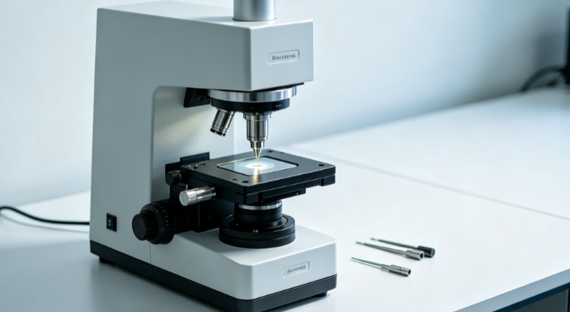
nanoindentation hardness Testing Services: Ultra‑Precision Mechanical Characterisation at the Nanoscale
As an independent third-party testing service provider, we offer specialised nanoindentation hardness testing for materials where conventional micro‑ or macro‑hardness methods (Vickers, Knoop, Rockwell, Brinell) are inadequate – including ultra‑thin films (< 100 nm), PVD/CVD coatings, DLC (diamond‑like carbon) layers, semiconductor wafers, MEMS devices, biomaterials (bone, dentine, cartilage), polymers, composites, ceramics, and individual microstructural phases. Nanoindentation is the premier technique for characterising mechanical properties at the nanoscale, using extremely low test forces (μN to mN range) and measuring indentation depths as shallow as a few nanometres. Our accredited laboratory follows international standards (ISO 14577, ASTM E2546) using state‑of‑the‑art nanoindentation instruments equipped with high‑resolution displacement sensors (< 0.01 nm) and force actuators (< 1 nN). This article outlines our nanoindentation testing capabilities – including scope, key test items, test methods, and standard compliance – to help manufacturers, R&D teams, and quality assurance professionals obtain precise nanomechanical characterisation for advanced materials and components.
1. What Is nanoindentation hardness Testing?
Nanoindentation, also known as instrumented indentation testing, is a depth‑sensing indentation technique that continuously records applied load and resulting penetration depth throughout the loading and unloading cycle. Unlike conventional hardness methods (Brinell, Rockwell, Vickers, Knoop) that require post‑test optical measurement of the indentation area, nanoindentation directly calculates mechanical properties from the load‑displacement curve using a diamond indenter of known geometry, typically a three‑sided pyramidal Berkovich tip with a curvature radius of approximately 50‑100 nm. The test involves pressing the indenter into the material surface under a precisely controlled load, holding at peak load to allow time‑dependent deformation, and then unloading while continuously monitoring depth. The resulting load‑displacement curve is analysed using established analytical frameworks—most notably the Oliver‑Pharr method—to extract hardness (H) and reduced elastic modulus (Er) without needing to measure the indentation optically. In nanoindentation, indentation depths (h) are ≤ 0.2 μm (200 nm), compared to macro‑scale depths of 2 N ≤ F ≤ 30 kN or micro‑scale depths where h > 0.2 μm (ISO 14577 classification). This ultra‑shallow penetration depth enables the characterisation of films as thin as a few tens of nanometres, individual microstructural phases, and materials with extremely small volumes, while minimising damage to delicate specimens. For the nano range, the mechanical deformation strongly depends on the real shape of the indenter tip, and the calculated material parameters are significantly influenced by the contact area function of the indenter used in the testing machine, requiring careful calibration of both instrument and indenter shape to achieve acceptable reproducibility between different machines.[reference:0][reference:1][reference:2]
2. Our Testing Scope for nanoindentation hardness
We cover a specialised range of materials, product forms, and test configurations where nanoscale mechanical characterisation is essential:
By material type / application: Thin films and coatings – PVD/CVD coatings (TiN, TiAlN, CrN, AlCrN, DLC – diamond‑like carbon), electroplated coatings (nickel, gold, silver), optical coatings (anti‑reflective, high‑reflectivity), protective coatings for MEMS devices, and nano‑laminate composites; Semiconductor wafers and microelectronics – silicon (crystalline and amorphous), GaAs, SiC, GaN, SiO₂, low‑k dielectrics, barrier layers (TaN, TiN), copper interconnects, solder bumps, and wafer dicing evaluation; Biomedical materials – bone, dentine, tooth enamel, cartilage, hydroxyapatite coatings, dental ceramics, implant surfaces, and hydrogel biomaterials; Polymers and soft materials – polyimide, photoresists, pressure‑sensitive adhesives, elastomers, and polymer thin films; Ceramics and hard coatings – alumina, zirconia, silicon carbide, tungsten carbide‑cobalt cermets, DLC coatings for cutting tools; Composite materials – interfacial and phase‑specific characterisation; MEMS and microstructures – micro‑gears, cantilevers, sensors, and actuator components; Individual microstructural phases – hardness of specific phases in multiphase alloys (e.g., carbides, intermetallic compounds); Metal glasses and amorphous alloys; Powder metallurgy components; Failure analysis – root cause investigation of coating delamination, brittle fracture, or surface degradation.
By test force range: Ultra‑low force: 0.001‑1 mN (for ultra‑thin films and sensitive biomaterials); Low force: 1‑100 mN (for general coatings and thin films); Medium force: 100‑500 mN (for thicker coatings, polymers, and small bulk specimens); Extended high‑force nanoindentation: up to 10 N (by arrangement for bulk materials).[reference:3][reference:4]
By specimen configuration: Flat polished surfaces (mirror finish, Ra ≤ 5 nm) – standard for accurate nanoindentation; Curved or irregular surfaces – using specialised sample holders and careful levelling; Cross‑sectional specimens – for through‑thickness hardness profiling of coatings and layered structures; Micro‑sections mounted in resin (25 mm or 30 mm diameter); Small or delicate components – requiring minimal contact force and precise positioning; Thin foils and films on substrates – requires appropriate load selection to avoid substrate influence.
By test environment: Laboratory testing (controlled temperature 23±2°C, vibration‑isolated base, active damping); Elevated temperature testing – up to 800°C (by arrangement); Low temperature testing – down to -150°C (by arrangement); Humidity‑controlled environment (< 40 % RH) for moisture‑sensitive materials.
3. International Standards & Compliance
All nanoindentation tests are performed in strict accordance with the following international standards:
ISO 14577‑1 (Metallic materials – Instrumented indentation test for hardness and other materials parameters – Part 1: Test method) – Specifies the method for determination of hardness and other materials parameters across three ranges: macro range (2 N ≤ F ≤ 30 kN), micro range (F < 2 N, h > 0.2 μm), and nano range (h ≤ 0.2 μm). This international standard applies to thin metallic and non‑metallic coatings and non‑metallic materials, requiring careful calibration of both instrument and indenter shape for acceptable reproducibility in the nano range.
ASTM E2546 (Standard practice for instrumented indentation testing) – The primary US standard covering requirements for generating data to determine indentation hardness and other material properties across nano, micro, and macro scales using instrumented indentation testing (IIT).
ISO 14577‑2 (Verification and calibration of testing machines).
ISO 14577‑3 (Calibration of reference blocks).
ISO 14577‑4 (Test method for metallic and non‑metallic coatings).
ASTM E384 (Standard test method for microindentation hardness of materials) – The primary US standard covering Vickers and Knoop microhardness testing with loads from 1 gf to 1000 gf, also applicable to nanoindentation calibration and verification procedures.
ISO 6507‑1 (Metallic materials – vickers hardness test – Part 1: Test method) – For cross‑referencing macro‑scale hardness values with nanoindentation data.
GB/T 4340.1 (Metallic materials – vickers hardness test – Part 1: Test method) – Chinese national standard for comparison and traceability.
GB/T 18449.1 (Metallic materials – knoop hardness test – Part 1: Test method).[reference:5][reference:6][reference:7]
4. Key Test Items & Measurement Parameters
Our nanoindentation testing services produce detailed, high‑precision nanomechanical data for advanced materials and coatings. Key parameters and deliverables include:
nanoindentation hardness (H) – The most fundamental nanomechanical property, representing a material‘s resistance to plastic deformation at the nanoscale. Calculated using the Oliver‑Pharr method as H = Pmax / Ac, where Pmax is the peak applied load and Ac is the projected contact area derived from the indenter geometry function. For homogeneous materials, hardness is typically load‑independent in the nano range. For thin coatings and surface layers, hardness increases as indentation depth decreases (smaller volumes contain fewer defects), revealing the intrinsic strength of the material. Accuracy is validated using certified reference materials such as fused silica (H = 9.25 GPa) with a typical measurement precision of ±5 %.
elastic modulus (Young‘s modulus – E) – Represents the material’s resistance to elastic (recoverable) deformation at the nanoscale. Extracted from the initial slope of the unloading curve, known as the contact stiffness (S = dP/dh), using the formula Er = (√π / (2β)) × (S / √Ac), where β is a geometric factor (≈ 1.034 for Berkovich indenters). The reduced elastic modulus Er is calculated first, then converted to the true Young‘s modulus E using the relationship 1/Er = (1‑ν²)/E + (1‑νᵢ²)/Eᵢ, where ν is Poisson’s ratio of the specimen and Eᵢ and νᵢ are elastic properties of the diamond indenter (Eᵢ = 1141 GPa, νᵢ = 0.07). For isotropic elastic materials, the nanoindentation modulus agrees well with bulk values.
Continuous stiffness measurement (CSM) – Advanced dynamic mode where a small sinusoidal oscillation (typically 1‑200 Hz) is superimposed on the quasi‑static loading signal. This enables continuous monitoring of contact stiffness and calculation of elastic modulus and hardness as functions of indentation depth – producing a “property‑versus‑depth” profile through layered structures, thin films, coatings, or gradients. CSM can also separate elastic and plastic components and detect phase transformations, delamination, and cracking events during the indentation process.
Fracture toughness (KIC) – For brittle materials such as ceramics, glasses, and hard coatings, fracture toughness is measured using a cube‑corner diamond indenter (sharp 90° corner). Indentation‑induced cracks propagate from the corners; the crack length is measured optically and KIC is calculated using established formulae (e.g., Palmqvist or Evans). Results are critical for evaluating the resistance of brittle coatings to fracture and spallation.
Creep behaviour – Time‑dependent plastic deformation under constant load. Measured by holding the indenter at peak load for a specified dwell time (typically 30‑300 seconds) while monitoring depth increase over time. The creep strain rate dε/dt is calculated from the displacement‑time data. For polymers and biological materials, creep behaviour characterises viscoelastic relaxation and stress recovery after unloading.
Storage modulus (E‘) and loss modulus (E″) – For viscoelastic materials (polymers, biomaterials, gels), dynamic nanoindentation (DMA mode) separates the elastic and viscous components. E‘ represents the stored (elastic) energy, while E″ represents the dissipated (viscous) energy. The loss factor tan δ = E″ / E‘ indicates damping characteristics.
Plastic work and elastic work – Calculated from the area under the loading curve (total work) minus the area under the unloading curve (recovered elastic work). The plastic work fraction (Wplastic / Wtotal) indicates the material’s capacity for energy dissipation during indentation.
Strain rate sensitivity (m) – Measures how hardness changes with loading rate. Determined by performing indentations at multiple loading rates (e.g., 0.05‑5 mN/s) and fitting the relationship H ∝ ε̇ᵐ, where ε̇ is the strain rate. Higher m values indicate greater rate‑dependent plasticity.
Interface adhesion strength / delamination – For coatings and thin films, nanoindentation can assess the adhesion strength of the coating‑substrate interface. Indentation near the interface causes delamination or buckling; the critical load for delamination is recorded. For quantitative measurement, scratch testing mode (using a ramp load) measures the critical load for cohesive or adhesive failure. Combining nanoindentation with automated grid mapping (indentation array) can generate 2D maps of hardness and modulus across heterogeneous surfaces.
5. Test Procedure & Specifications
Our laboratory strictly adheres to the requirements of ISO 14577 and ASTM E2546. The key steps and specifications are summarised below:
Specimen preparation – The test surface must be flat and highly polished to a mirror finish (Ra ≤ 5 nm) to ensure accurate contact detection and minimise roughness‑induced variability. Surface roughness is verified by AFM or optical profilometry. For polymers and biomaterials, softer polishing protocols are used to avoid embedding abrasives or inducing residual stress. The specimen is cleaned ultrasonically (sequential baths in isopropanol, acetone, and deionised water) to remove dust, oils, and organic contaminants. For cross‑sectional profiling, specimens are mounted in epoxy or acrylic resin and polished to a mirror finish.
Indenter selection – The standard nanoindentation indenter is a diamond Berkovich three‑sided pyramidal tip (half‑angle 65.3°), valued for its well‑defined geometry and sharpness (apex radius ≈ 50‑100 nm). This design eliminates the truncation issues associated with four‑sided Vickers tips. For fracture toughness measurements, a cube‑corner indenter (90° corner angle) is employed for its ability to induce crack propagation at lower loads. For spherical indentation (elasticity measurements at low loads), tungsten carbide or diamond spherical tips (R = 10‑100 μm) are available.
Contact calibration (zero‑point determination) – Before each test or test series, the indenter is slowly brought into contact with the specimen surface until a contact trigger force (typically < 1 μN) is detected. The position sensor records the initial contact depth, establishing the zero‑point. For rough or curved surfaces, a more sophisticated approach with step‑by‑step approach and touchdown detection is used.
Indentation parameters – Load control mode is typically used for coating and thin film testing, ensuring that the indentation remains within a specified depth limit; displacement control is preferred for bulk materials with known hardness. Standard loading rates range from 0.05‑5 mN/s (softer materials use lower rates). The dwell time at peak load is typically 5‑60 seconds; for creep‑sensitive materials or viscoelastic polymers, dwell times of 60‑300 seconds are employed.
Thermal drift correction – Because nanoindentation displacement resolution is in the sub‑nanometre range, thermal drift must be carefully managed. Before each test series, the indenter is held out of contact (withdrawn) and the position signal is monitored for 60‑120 seconds to calculate the drift rate (nm/s). The drift is then subtracted from all subsequent depth measurements. The laboratory is maintained at 23±2°C with temperature fluctuations ≤ ±0.5°C, and the instrument is placed on a vibration‑isolated table.
Indentation spacing – To avoid interaction between adjacent indentations (work‑hardening or residual stress effects), the distance between indentation centres must be at least 15‑20 times the maximum indentation depth. Typical spacing is ≥ 5‑10 μm for shallow indentations (< 100 nm depth). The distance from any indentation to the specimen edge must be ≥ 5 times the indentation diameter.
Number of indentations – For quality control and statistical confidence, a minimum of 5 indentations are performed for each test condition (different loads, locations, or specimens). The mean and standard deviation of hardness and modulus are reported. For mapping studies (grid arrays), 100‑1,000 indentations may be performed.
Calibration & verification – The nanoindenter is calibrated daily using a certified reference sample (e.g., fused silica) with known reduced modulus (Er = 69.6 GPa) and hardness (H = 9.25 GPa). The indenter‘s area function Ac(hc) – the relationship between contact depth and projected contact area – is determined by performing indentations on a reference material over a range of depths. This area function is then used to calculate hardness and modulus for all subsequent tests. The measurement system (capacitive displacement sensor) and force transducer are calibrated annually by an accredited metrology laboratory per ISO 14577‑2.
6. Typical Applications & Suitable Materials
nanoindentation hardness testing is essential for the following advanced material applications:
PVD/CVD coatings (TiN, TiAlN, CrN, DLC – diamond‑like carbon) – For cutting tools, wear‑resistant surfaces, and decorative coatings. Nanoindentation with very low loads (1‑10 mN) ensures that the indentation depth remains within the coating (≤ 10 % of coating thickness), providing true coating‑only hardness without substrate influence. Hardness values of 20‑40 GPa for TiN/TiAlN and up to 50‑80 GPa for DLC are typical. The technique also detects defects, porosity, and non‑uniform hardness.
Semiconductor wafers (Si, GaAs, SiC, SiO₂, low‑k dielectrics) – In microelectronics fabrication, nanoindentation characterises the mechanical properties of dielectric films, barrier layers (TaN, TiN), and interconnect metals (Cu, W) in integrated circuits. Film modulus and hardness directly affect the control of the chemical mechanical planarisation (CMP) process and package‑level reliability.
Thin coatings on soft substrates – Nanoindentation is essential for evaluating hard coatings applied to soft substrates (e.g., DLC on polymer, anti‑scratch coatings on plastic lenses). By keeping indentation depths shallow (< 10 % of coating thickness), the true coating hardness is obtained without substrate influence.
Thermal barrier coatings (TBC) for aerospace – Turbine components rely on yttria‑stabilised zirconia (YSZ) coatings to insulate metal substrates from combustion temperatures. Nanoindentation maps the evolution of TBC properties after thermal cycling, detecting sintering‑induced stiffening and degradation before visible spallation occurs.
Biomaterials (bone, dentine, cartilage, hydroxyapatite coatings) – Nanoindentation characterises the modulus of individual osteons, trabeculae, and hydroxyapatite crystals at scales inaccessible to macroscale testing. These measurements inform biomaterial design and implant surface engineering. The small indentation size (< 2 μm) permits testing of hydrated (wet) specimens in fluid cells.
MEMS devices and micro‑components – Micro‑gears, cantilevers, sensors, and actuator components are too small for conventional microhardness testing. Nanoindentation with μm‑scale indentation sizes (10‑50 μm diagonal) provides necessary data for material selection, quality control, and reliability prediction.
Individual phases in multiphase alloys – In tool steels, superalloys, and metal‑matrix composites, nanoindentation can selectively target individual phases (e.g., carbides, intermetallic compounds, ferrite, martensite) under high‑magnification optical imaging, obtaining phase‑specific hardness values.
Polymer and composite films – The surface mechanical properties of polymer coatings, adhesive films, and composite matrix materials are characterised by nanoindentation using low loads (0.1‑5 mN) and spherical indenters to obtain modulus, hardness, creep, and viscoelastic relaxation data. Continuous stiffness measurement (CSM) provides depth‑dependent profiling through multilayer film stacks.
Metal glasses and amorphous alloys – Nanoindentation measures nanoscale hardness and elastic modulus of bulk metallic glasses and amorphous ribbons. The data help evaluate shear band formation, ductility, and thermal stability.
Research & failure analysis – Nanoindentation is used to assess individual microstructural phases, evaluate decarburised layers (< 100 μm), map hardness across welded zones and heat‑affected zones, and determine residual stress distributions through the surface layer.
7. Advantages & Limitations of nanoindentation hardness Testing
Understanding the strengths and limitations of nanoindentation ensures proper application and interpretation of results.
Advantages: Enables measurement of films as thin as 20‑50 nm (the true breakthrough capability of the technique). Continuous depth monitoring eliminates the need for optical measurement of indentation area – a major source of error in conventional microhardness methods. The load‑displacement curve yields hardness, elastic modulus, creep, fracture toughness, and viscoelastic properties from a single test – far more data than Vickers or Knoop methods. The technique is minimally destructive – the indentation size is typically 1‑10 μm, often invisible or acceptable on finished components. The technique can characterise soft biomaterials, gels, polymers, and rubbers using spherical indenters and low loads (0.01‑1 mN). Continuous stiffness measurement (CSM) provides depth‑resolved profiling through coatings and layered structures. Nanoindentation is excellent for small samples, micro‑components, and localized regions.
Limitations: Requires mirror‑finished surfaces (Ra ≤ 5 nm); rough surfaces produce highly scattered data and invalid indentation shapes. The instrument is expensive and requires skilled operation and regular calibration using reference materials. The test is relatively slow per indentation (30‑60 seconds) plus mapping time (minutes to hours). Inherent indentation size effect (ISE) means that apparent hardness may vary with load for very shallow depths (< 100 nm), requiring careful interpretation. Substrate influence may still be present if indentation depth exceeds 10 % of coating thickness – requires finite element modelling for correction. For anisotropic materials (single crystals, oriented polymers), results must be interpreted with caution. Cannot be used for extremely soft materials (< 0.01 GPa) or extremely hard materials (> 120 GPa) without indenter damage.
8. Reporting & Result Presentation
Our test reports are detailed, transparent, and compliant with ISO/IEC 17025, ISO 14577, and ASTM E2546. Each report includes:
Specimen identification – Material type, coating specification (if applicable), component description, sampling location, orientation (for anisotropic materials), and preparation method (mounting, polishing, cleaning).
Test conditions – Standard referenced (ISO 14577‑1, ASTM E2546), indenter type (Berkovich, cube‑corner, spherical, etc.), test force or depth parameters, loading/unloading rates (mN/s), dwell time at peak load (seconds), thermal drift rate (nm/s), temperature (23±2°C), humidity (< 40 % RH), and instrument model and serial number.
Individual indentation data – For each indentation: peak load Pmax (mN), maximum penetration depth hmax (nm), contact stiffness S (μN/nm), calculated hardness H (GPa), reduced modulus Er (GPa), and Young’s modulus E (GPa). For CSM tests, a hardness‑depth profile (hardness vs. depth) and modulus‑depth profile are included. For creep tests, displacement‑time curve during dwell is plotted.
Statistical summary – Mean hardness and modulus, standard deviation (SD), coefficient of variation (CV), number of valid indentations, and range (minimum to maximum).
Calibration records – Reference material used (e.g., fused silica), certified values (H = 9.25 GPa, Er = 69.6 GPa), measured average values, deviation (%), indenter area function calibration data, and date of calibration.
Mechanical property mapping (if requested) – 2D contour plots or colour maps of hardness and modulus across the specimen surface from automated grid indentation arrays (10×10 up to 50×50 grid points, spacing 10‑100 μm).
Equipment calibration status – Instrument model and serial number (e.g., Hysitron TI Premier, MTS Nano G200, KLA iMicro), date of last full verification, reference material traceability, and verification results.
Compliance statement – Pass/fail determination against customer specification, purchase order, or material standard.
9. Why Choose Our Third‑Party Nanoindentation Testing Services?
As an independent laboratory with specialised expertise in nano‑scale mechanical characterisation, we provide unbiased, accurate, and legally defensible nanomechanical data. Our strengths include:
ISO/IEC 17025 accreditation – Our nanoindentation testing is CNAS and CMA accredited, with regular participation in proficiency testing (e.g., ISO 14577, ASTM E2546 interlaboratory programmes).
Specialised nanoindentation instruments – We operate a fleet of fully automated nanoindentation systems: KLA iMicro NanoIndenter (0.001‑1000 mN force range, 0.001 nm displacement resolution, integrated optical microscope), Hysitron TI 950 (high precision for biomaterials and soft polymers, < 0.1 nN resolution, environmental chamber for controlled humidity), MTS Nano Indenter G200 (500 mN maximum load, high‑speed scan capability, CSM module). All instruments feature low‑drift temperature control (0.5°C stability), vibration isolation (active and passive), and closed‑loop force/displacement control.
Comprehensive indenter tip library – Berkovich (standard nano‑scale hardness and modulus), cube‑corner (fracture toughness), spherical (elasticity, creep, soft materials), Vickers (micro‑scale correlation), and custom‑designed tips for specialised applications.
Environmental control – Testing performed at 23±2°C / 40‑50 % RH (standard); heated stage (up to 800°C) for thermal nanoindentation; cooling stage (down to -150°C) for cryogenic testing; liquid cell for hydrated biomaterials and soft gels; humidity control (< 40 % RH) for moisture‑sensitive materials.
Thin coating and film expertise – For ultra‑thin films (< 100 nm), we select test forces of 0.01‑1 mN and utilise CSM mode to ensure that indentation depths remain within the coating layer. We also perform and report substrate‑effect analysis when required.
Fast turnaround – Routine nanoindentation (5‑10 indentations) typically completed within 2‑3 business days. Grid mapping studies (25‑100 indentations) within 3‑5 business days. Full CSM profile (load‑on‑depth curve) and creep analysis within 5‑7 business days.
Detailed reporting – Reports include load‑displacement curves, individual indentation data, statistical summaries, calibration records, indentation images (SEM or optical micrographs of selected indents), and clear pass/fail conclusions against customer specifications.
Confidentiality – Full protection of your material composition, coating recipes, component geometry, and R&D objectives.
Consultative support – Our materials scientists and nanoindentation specialists assist with parameter selection (loading profile, maximum force, dwell time), specimen preparation (polishing, mounting, cleaning), data interpretation (size effects, substrate influence, creep behaviour), and root‑cause analysis of nanoscale mechanical failures.
Get Started with Your Nanoindentation Testing Project
Contact our team with your material type (coating, semiconductor, biomaterial, ceramic, polymer, composite), required nanomechanical parameters (hardness, modulus, creep, fracture toughness, CSM profile), estimated coating thickness (for thin films), specimen dimensions, and applicable standard (ISO 14577, ASTM E2546, or custom). We will provide a detailed quotation, sample preparation guidelines (including surface polishing requirements, minimum specimen size, and recommended cleaning protocols), and a testing schedule. Let us help you obtain precise, nanoscale mechanical property data for advanced materials research, quality control, and product development.
This article provides an overview of our nanoindentation hardness testing capabilities. For specific test methods, sample quantity, and pricing, please request a tailored service proposal.