Reasons for choosing our testing services
ZHONGXI Testing has obtained inspection qualification certifications from multiple countries and regions worldwide. We possess a senior testing team and advanced testing methods, providing independent, impartial, and professional third-party verification services for global carbon projects.
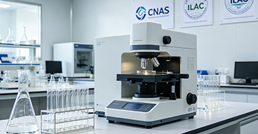
Internationally recognized authority
Certified by multiple international standards such as CNAS, VCS, and GS, with reports universally applicable worldwide.

Global service capability
Covering 140+ countries and regions, it supports on-site detection and remote verification in multiple languages.
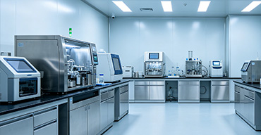
Professional experimental methods
Adopt standard experimental methods to ensure accurate and reliable data.
Comprehensive Analytical Testing of Transparent Conductive Glass: Advanced Characterisation for Display, Photovoltaic, and Smart Window Applications
Transparent conductive glass (TCG)—typically coated with indium tin oxide (ITO), fluorine‑doped tin oxide (FTO), aluminium‑doped zinc oxide (AZO), or silver nanowire networks—is an essential component in touchscreens, solar cells, OLED lighting, smart windows, and electromagnetic interference (EMI) shielding. The performance of TCG relies on a delicate balance of sheet resistance, optical transmittance, haze, surface roughness, coating uniformity, adhesion, and chemical durability. Even minor deviations in coating thickness or post‑treatment can lead to non‑uniform conductivity, reduced light extraction, poor device yield, or premature failure. Our laboratory offers a fully integrated, multi‑technique testing platform specifically designed for the rigorous characterisation of transparent conductive glass, combining electrical measurements (four‑point probe, van der Pauw), optical spectroscopy (UV‑Vis‑NIR, haze meter), surface topography (AFM, profilometry), coating adhesion (tape test, scratch test), and environmental durability testing. We deliver quantitative, diagnostic, and predictive data that supports material development, quality control, supplier qualification, and regulatory compliance for the electronics, automotive, building, and energy sectors.
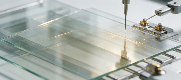
Why Comprehensive Testing of Conductive Glass Is Critical for Device Performance and Yield
Manufacturers and end‑users seeking TCG testing often encounter challenges such as unacceptable sheet resistance non‑uniformity, batch‑to‑batch variations in optical clarity, or rapid degradation of conductivity under humidity or heat. These issues frequently arise from sub‑optimised sputtering or chemical deposition processes, inadequate post‑annealing, or surface contamination from handling. Furthermore, the interaction between the conductive layer and the glass substrate—including thermal expansion mismatch and chemical interactions—can lead to delamination or stress‑induced cracking in long‑term service. Our service provides a systematic characterisation that quantifies sheet resistance (Ω/□), average transmittance (%, including visible and NIR), haze (%), surface roughness (Ra, Rq), coating thickness (nm), adhesion rating, and environmental stability (after humidity, salt spray, and temperature cycling). By identifying the root causes of performance deviations—such as insufficient oxygen partial pressure, grain boundary scattering, or surface segregation of dopants—we enable clients to optimise deposition parameters, implement effective cleaning protocols, and ensure batch‑to‑batch consistency for high‑reliability products.
Our Analytical Capabilities: From Electrical and Optical Properties to Durability Assessment
Our testing framework is structured into five interconnected modules, each addressing a critical aspect of TCG quality and application fitness:
Electrical characterisation—We measure sheet resistance using a calibrated four‑point probe with precision current sources and voltmeters, providing uniformity mapping across the glass surface (typically 5‑25 points) to identify spatial variations. For patterned or anisotropic films, we apply the van der Pauw method to determine resistivity and Hall effect for carrier concentration and mobility. Temperature‑dependent resistance (25‑200 °C) is measured to assess thermal stability and the semiconductor‑like behaviour of TCO layers. Contact resistance and line resistance are evaluated using transfer length method (TLM) structures where applicable.
Optical and visual characterisation—We measure total and diffuse transmittance over the wavelength range 200‑2500 nm (UV‑Vis‑NIR) using a double‑beam spectrophotometer with an integrating sphere, providing average transmittance (Tavg) in visible (400‑700 nm) and NIR regions. Haze is quantified with a dedicated haze meter according to ASTM D1003. Colour coordinates (CIELAB, a*, b*, L*) are derived to assess neutral appearance. Reflectance and absorption are also reported, enabling calculation of the figure of merit (e.g., σDC/σopt). For anti‑reflective or textured coatings, we perform angle‑resolved scattering measurements.
Surface morphology and coating integrity—We use atomic force microscopy (AFM) in tapping mode to image surface topography and calculate roughness (Ra, Rq) and grain size. White light interferometry provides large‑area step height and flatness. Scanning electron microscopy (SEM) with energy‑dispersive X‑ray spectroscopy (EDS) confirms elemental composition and detects defects (pin‑holes, particles). X‑ray photoelectron spectroscopy (XPS) probes the surface chemistry and oxidation states of the conductive layer. Coating thickness is cross‑sectioned by focused ion beam (FIB)‑SEM or measured by spectroscopic ellipsometry for non‑destructive optical modelling.
Adhesion and mechanical durability—We perform cross‑hatch tape test (ASTM D3359) and scotch tape peel test to assess coating adhesion. Scratch testing with a diamond tip under progressive load determines critical load for delamination. taber abrasion and steel wool rub tests (with controlled pressure and cycles) evaluate resistance to wear, simulating cleaning and handling. Micro‑hardness is measured using nanoindentation.
Environmental and long‑term stability—We subject TCG samples to damp heat (85 °C / 85 % RH) for 100‑1000 hours (IEC 61215), thermal cycling (‑40 °C to +85 °C), and salt spray (5 % NaCl, 35 °C) testing. Performance is re‑evaluated periodically to determine ageing effects on sheet resistance, transmittance, and appearance. We also perform UV exposure tests (UVA/B) to assess photodegradation. Chemical resistance to common solvents, acids, and alkalis is assessed by immersion and subsequent measurement.
High‑Level Diagnostics and Predictive Correlative Analysis
We integrate electrical, optical, and morphological data to build structure‑property‑performance relationships—for example, correlating grain size (AFM) with sheet resistance (via grain‑boundary scattering), or roughness with optical haze. Our multivariate statistical analysis (PCA, PLS) identifies critical quality attributes (CQAs) that govern device performance, enabling quality‑by‑design (QbD) strategies for process control and scale‑up. For failure analysis, we combine post‑ageing characterisation (XPS, SEM, AFM) with degradation trends to differentiate between surface oxidation, interdiffusion, stress‑induced cracking, and moisture‑induced corrosion.
Regulatory Compliance and Quality Assurance
All test methods align with ASTM D1003 (haze), ASTM F390 (sheet resistance), ISO 13314 (abrasion), and IEC 61215 (environmental testing for photovoltaics). Our laboratory holds ISO/IEC 17025:2017 accreditation for a broad scope of electrical, optical, and environmental testing. We issue certified test reports with full measurement uncertainty, traceability to NIST/SRM standards, and quality control data (reference samples, blanks, duplicates). For automotive or building product certification (e.g., IEC 61730, ECE R43), we provide comprehensive data packages with detailed protocols and raw data archives.
Our Distinctive Advantages in Transparent Conductive Glass Testing
Comprehensive figure‑of‑merit assessment: We go beyond simple sheet resistance and transmittance by calculating the Haacke figure of merit (ΦTC) and other quality indices, providing a single performance metric that combines electrical and optical properties—critical for benchmarking and material selection.
Correlative multi‑technique mapping: We perform sheet resistance mapping (four‑point probe), optical mapping (spectrophotometry), and surface topography (AFM/profilometry) on identical areas, enabling direct correlation between local defects, conductivity, and optical clarity—a powerful diagnostic tool for yield improvement.
Realistic environmental simulation: Our environmental chambers are equipped for combined humidity, temperature, and UV cycling, mimicking real‑world outdoor/indoor conditions more faithfully than single‑stress tests. This provides predictive data for long‑term reliability.
Expert interpretation and process guidance: Our team includes materials scientists and thin‑film specialists with extensive experience in TCO deposition. We provide specific, actionable recommendations—for example, suggesting optimal annealing conditions to reduce sheet resistance without increasing haze, or advising on oxygen‑argon ratio adjustments during sputtering.
Fast turnaround with flexible sample formats: Our standard full characterisation package is delivered within 7‑10 working days, with expedited 48‑hour screening for key parameters (sheet resistance, transmittance, haze). We accept whole panels, coupons, and patterned substrates, handling sizes from 1 cm² to 2 m².
End‑to‑End Service Workflow
We begin with a complimentary technical consultation to define your application requirements (display, PV, automotive, etc.), critical attributes, and regulatory needs. We design a tailored test plan, including sampling and handling guidelines. Upon sample receipt, we perform visual inspection and preconditioning. All tests are executed with strict QA/QC—reference standards, blanks, and duplicates. Data are integrated and reviewed by our lead scientist, then compiled into a comprehensive report containing sheet resistance maps, transmittance spectra, AFM images, environmental test profiles, and a clear executive summary with optimisation recommendations. A post‑report meeting is offered to discuss findings and guide process adjustments.
Partner with Us for Uncompromised Quality and Performance in Conductive Glass
Transparent conductive glass is a critical enabler for modern optoelectronics, and its reliability depends on rigorous, multi‑dimensional characterisation. Our testing service provides the scientific depth, practical relevance, and regulatory support necessary to ensure your material meets the highest standards. We have supported leading display manufacturers, solar cell producers, and smart window developers in optimising their TCG processes.
We invite you to contact our technical experts to discuss your specific testing needs—whether for incoming material inspection, process development, or failure analysis. With our advanced analytical instruments, accredited protocols, and specialised expertise, we provide the clarity and confidence you need to drive innovation. Request a detailed proposal or schedule a technical consultation today and take the next step towards superior transparent conductive glass solutions.