Reasons for choosing our testing services
ZHONGXI Testing has obtained inspection qualification certifications from multiple countries and regions worldwide. We possess a senior testing team and advanced testing methods, providing independent, impartial, and professional third-party verification services for global carbon projects.

Internationally recognized authority
Certified by multiple international standards such as CNAS, VCS, and GS, with reports universally applicable worldwide.

Global service capability
Covering 140+ countries and regions, it supports on-site detection and remote verification in multiple languages.

Professional experimental methods
Adopt standard experimental methods to ensure accurate and reliable data.
Comprehensive LED Thin-Film Chip Testing Services – Advanced Characterization for Micro-LED, Thin-Film Flip-Chip, and Wafer-Level Devices
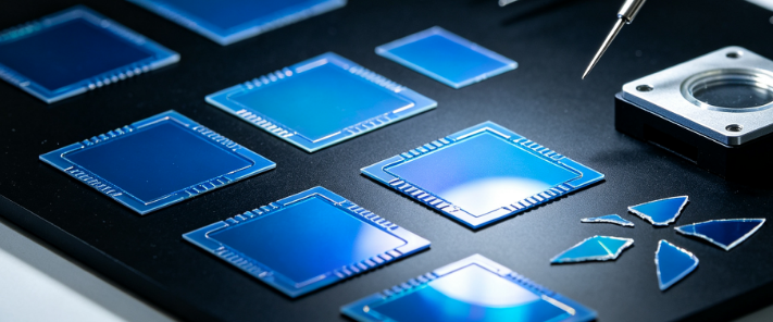
LED thin-film chips represent the forefront of solid-state lighting and display technology, enabling ultra-thin form factors, enhanced light extraction, improved thermal management, and compatibility with flexible substrates. These devices – including thin-film flip-chip (TFFC) LEDs, micro-LEDs (μLEDs), vertical thin-film LEDs, and wafer-level chip-scale packages (WLCSP) – are fabricated by removing the growth substrate and bonding the epitaxial stack to a carrier, followed by chip singulation and sidewall passivation. The performance of these chips is governed by a complex interplay of epitaxial quality, thin-film thickness, surface texturing, current spreading, sidewall passivation, and bonding interface integrity. Clients seeking LED thin-film chip testing services typically aim to: (i) verify electro-optical performance at the chip level before packaging, (ii) characterize wavelength uniformity and efficiency across the wafer, (iii) evaluate the impact of thin-film processing on internal quantum efficiency and light extraction, (iv) detect defects such as micro-cracks, delamination, and current crowding, and (v) generate comprehensive qualification data for display manufacturers, automotive OEMs, and micro-LED integrators. Our laboratory offers a fully integrated, ISO/IEC 17025‑accredited LED thin-film chip testing service that combines wafer-level probing, high-resolution electroluminescence mapping, micro-photoluminescence, spectral analysis, current-voltage characterization, thermal imaging, and advanced failure analysis into a unified assessment platform. We do not merely report pass/fail results; we deliver a holistic chip performance fingerprint that correlates epitaxial structure, thin-film processing, and chip architecture with real-world behaviour, empowering our clients to accelerate development, improve yield, and achieve competitive differentiation in the rapidly evolving LED market.
Why Professional LED Thin-Film Chip Testing Is Indispensable for Display and Lighting Applications
Thin-film LED chips are significantly more complex than conventional lateral chips. The removal of the sapphire growth substrate introduces new failure modes: epitaxial layer cracking due to stress relaxation, bonding void formation at the carrier interface, sidewall leakage from incomplete passivation, and wavelength shifts from strain redistribution. For micro-LED displays, where chip dimensions approach 5–10 μm, edge effects dominate performance, and a single defective emitter can cause a visible pixel failure. For automotive lighting, reliability under extreme temperatures and humidity is non-negotiable. Regulatory and industry standards such as IES LM‑80, LM‑79, JEDEC JESD22, AEC‑Q102, and ISO 14707 impose stringent requirements on testing methods and data reporting. Our testing services provide the objective evidence needed to demonstrate conformity, support design allowables, and win certification. We help clients navigate the complex landscape of standards, ensuring that every thin-film chip meets the requirements of its intended application and regulatory jurisdiction.
Wafer-Level Probing and Electro-Optical Characterization – High-Throughput Chip Screening
The first step in thin-film chip qualification is wafer-level probing, which enables rapid screening of thousands of individual devices before dicing and packaging. Our automated probe station (Cascade Summit 12000) is equipped with a high-density probe card capable of contacting chips with pitches down to 20 μm, and a source-measure unit (Keysight B1500A) for precise current-voltage characterization. We perform forward voltage (VF) measurements at multiple current densities (from 0.1 A/cm² to 100 A/cm²), extracting ideality factor, series resistance, and reverse Leakage Current. For each chip, we record the electroluminescence (EL) intensity using a calibrated photodiode or a high-sensitivity camera, enabling the generation of wafer-level maps of radiant flux, peak wavelength, and forward voltage. Our proprietary binning software classifies chips according to user-defined performance criteria, providing yield statistics and spatial defect patterns. We also perform pulsed I-V measurements with pulse widths down to 100 ns to separate self-heating effects from intrinsic device performance, which is critical for micro-LEDs operating at high current densities.
High-Resolution Electroluminescence Mapping and Spectral Analysis – Wavelength Uniformity and Color Purity
For display and lighting applications, wavelength uniformity and color purity are paramount. Our high-resolution EL mapping system combines a microscope-based spectroradiometer (Instrument Systems CAS 140D) with a motorized XY stage, enabling point-by-point spectral acquisition with a spatial resolution of 1 μm. We measure peak wavelength (λp), dominant wavelength (λd), full width at half maximum (FWHM), and spectral power distribution (SPD) across the entire chip or wafer, generating 2D maps of wavelength shift, intensity variation, and color coordinates (CIE 1931 and 1976). For micro-LED displays, we quantify color gamut and color uniformity across the emitter array, identifying any systematic gradients or localized defects that could cause visible mura. We also perform temperature-dependent EL measurements from −40 °C to +150 °C to determine the wavelength shift coefficient (nm/K) and the efficiency droop behaviour, which are essential for predicting performance in real-world operating conditions.
Internal Quantum Efficiency (IQE) and Light Extraction Efficiency (LEE) – Separating Loss Channels
Total efficiency is the product of IQE, LEE, and electrical injection efficiency. To diagnose the limiting factor in thin-film chips, we offer temperature-dependent photoluminescence (PL) and electroluminescence (EL) measurements. Our PL system uses a 266 nm or 325 nm laser, a cryostat (4 K to 300 K), and a high-resolution spectrograph. By comparing the integrated PL intensity at 4 K (assuming near-unity IQE) with that at 300 K, we calculate the room-temperature IQE with an uncertainty of ±3%. For EL-based IQE, we measure the emission power at low temperature and low current, then extrapolate to room temperature using the ABC model. The light extraction efficiency is then estimated by comparing the EQE (from electrical measurement) with the IQE (from optical measurement), providing a clear picture of whether losses arise from non-radiative recombination (material quality) or photon trapping (chip design and surface texturing). We also perform angle-resolved EL using a goniometric stage to measure the far-field radiation pattern, from which we calculate the extraction efficiency into a defined cone and the total hemispherical extraction.
Micro-Photoluminescence and Cathodoluminescence Mapping – Defect Visualization at the Nanoscale
Thin-film LED chips are susceptible to nanoscale defects that can act as non-radiative recombination centers or current leakage paths. Our micro-photoluminescence (μ-PL) system combines a confocal microscope with a high-resolution spectrometer, achieving a spatial resolution of 0.5 μm. We map the PL intensity, peak wavelength, and linewidth across individual chips, revealing dark spots, wavelength inhomogeneities, and strain fields that are invisible in ensemble measurements. For even higher resolution, we employ cathodoluminescence (CL) in a scanning electron microscope (SEM) at 5–20 K, which provides spatial resolution down to 10 nm. Our CL system (Gatan MonoCL4) can acquire panchromatic and monochromatic images, as well as hyperspectral maps, enabling the correlation of radiative defects with specific structural features such as dislocations, stacking faults, or sidewall damage. These techniques are invaluable for optimizing epitaxial growth, thin-film bonding, and sidewall passivation processes.
Current-Voltage and Capacitance-Voltage Characterization – Electrical Integrity and Trapping Analysis
The electrical performance of thin-film chips is characterized by a suite of DC, pulsed, and AC measurements. We perform forward and reverse I-V measurements at multiple temperatures to extract the ideality factor, saturation current, series resistance, and shunt resistance. For micro-LEDs, we measure the current density vs. voltage (J-V) behaviour at high injection levels to identify the onset of efficiency droop and the contribution of Auger recombination. We also perform capacitance-voltage (C-V) measurements (1 kHz to 10 MHz) on Schottky or MIS structures to determine the built-in potential, depletion width, and interface trap density (Dit). For trapping analysis, we employ deep-level transient spectroscopy (DLTS) with a temperature range of 77 K to 500 K, identifying trap levels with activation energies, capture cross-sections, and concentrations. This is particularly valuable for detecting defects introduced during substrate removal, bonding, or sidewall etching. We also perform low-frequency noise measurements (1/f noise) to assess the density of traps and the quality of the active region.
Thermal Characterization and Junction Temperature Measurement – Managing Heat in Thin-Film Devices
Thin-film LED chips often operate at high current densities, making thermal management critical for efficiency and reliability. We perform thermal resistance (Rth) measurement using the transient thermal impedance method (T3Ster® system), which applies a step current and records the cooling curve of the forward voltage to derive the structure function and the cumulative thermal resistance network (junction-to-case, case-to-ambient). We also employ infrared (IR) thermography with a spatial resolution of 5 μm to map the temperature distribution across the chip under actual bias, identifying hot spots that may lead to local degradation. For micro-LEDs, we use Raman thermometry with a spatial resolution of 0.5 μm to measure the local temperature in the active region, providing unmatched accuracy for small devices. Our thermal analysis also includes thermal cycling (−40 °C to +150 °C, up to 2,000 cycles) to evaluate the thermal-mechanical fatigue of the bonding interface and sidewall passivation.
Reliability and Lifetime Testing – Accelerated Stress and Physics-of-Failure Modeling
Reliability qualification is a critical step for thin-film LED chips in automotive, display, and industrial applications. We operate a dedicated multi-site reliability test system capable of applying constant current, constant voltage, or pulsed stress to up to 96 devices simultaneously, with independent temperature control (up to 200 °C) and humidity (10–95% RH). We perform the following accelerated stress tests:
(i) High-temperature operating life (HTOL) – to evaluate the stability of the active region and contacts.
(ii) High-temperature reverse bias (HTRB) – to assess the integrity of the passivation and the bonding interface.
(iii) Wet high-temperature operating life (WHTOL) at 85 °C/85% RH – to evaluate moisture resistance and electrochemical migration.
(iv) Thermal cycling and thermal shock – to assess the mechanical robustness of the thin-film stack and bonding.
(v) ESD (HBM and CDM) per ANSI/ESDA/JEDEC standards to assess robustness.
During stress, we periodically measure EL intensity, forward voltage, and wavelength to monitor degradation. We analyze the degradation kinetics using Arrhenius, Eyring, and power-law models, extracting the activation energy (Ea) and the lifetime (L10, L50) at use conditions. Our proprietary physics-of-failure (PoF) framework combines experimental data with TCAD simulations to identify the dominant failure mechanisms (e.g., contact degradation, defect propagation, or passivation breakdown) and to provide guidelines for derating or design improvement.
Advanced Failure Analysis and Root-Cause Diagnostics
When thin-film LED chips fail to meet specifications or exhibit unexpected degradation, our failure analysis (FA) service provides a systematic, multi-technique investigation. Our FA flow includes:
(i) Optical and confocal microscopy for visual inspection of surface damage, discoloration, and macro-defects.
(ii) Scanning electron microscopy (SEM) with EDS for high-magnification imaging and elemental analysis of defects, contamination, and bonding interfaces.
(iii) Focused ion beam (FIB) cross-sectioning combined with TEM and SAED to examine the epitaxial stack, bonding interface, and sidewall passivation at the atomic scale.
(iv) Electron-beam-induced current (EBIC) and cathodoluminescence (CL) mapping to locate recombination centers and correlate them with structural defects.
(v) Infrared (IR) thermography and Raman thermometry to identify hot spots and thermal failure pathways.
We integrate all FA data with the chip's fabrication and testing history to construct a complete failure timeline, attributing the root cause to specific process steps, material quality, or handling procedures. This level of diagnostic depth is rarely available in commercial test houses and is highly valued by clients involved in yield improvement, supplier qualification, and technology transfer.
Our Distinctive Competencies – Integration, Expertise, and Global Compliance
What sets our LED thin-film chip testing service apart is the seamless integration of wafer-level probing, electro-optical characterization, defect mapping, thermal analysis, and reliability testing within a single laboratory, enabling correlative analysis that is impossible when samples are shipped between multiple vendors. Our team comprises PhD-level device physicists, materials scientists, and engineers with extensive experience in III-nitride epitaxy, thin-film processing, and micro-LED technology. We do not simply report numbers; we interpret them in terms of epitaxial quality, process integration, and device physics – for example, distinguishing between efficiency droop caused by Auger recombination versus current crowding, or identifying the root cause of wavelength shift as strain relaxation versus composition pulling.
Our laboratory is ISO/IEC 17025 accredited for a wide range of LED test methods, and we maintain NIST-traceable calibrations for all equipment. We participate in international round-robins (e.g., NIST, PTB, CIE) to ensure global comparability. We offer rapid turnaround – typically 3–5 business days for standard testing packages, with expedited options available – and we accept samples in various forms: full wafers (up to 200 mm), diced chips on carrier tape, and packaged devices. Our data analytics platform employs machine learning to identify subtle correlations between process parameters and chip performance, accelerating yield improvement and process optimization.
We also provide custom test plans for emerging thin-film LED architectures (e.g., micro-LEDs, nanowire LEDs, quantum-dot LEDs, and flexible LEDs) and for specific applications (e.g., AR/VR displays, automotive headlamps, and visible light communication). Our consulting services include material selection, process integration, certification strategy, and failure analysis with root-cause determination. We offer on-site sampling and mobile testing units for large-scale wafer fabs, ensuring that critical measurements can be performed without transport delays.
Comprehensive Service Modules – Tailored to Your Chip Type and Application
We organize our testing into modular packages to meet diverse client objectives:
Module 1 – Wafer-Level Probing and Binning: Automated VF, leakage, and EL intensity mapping with yield statistics – essential for production screening.
Module 2 – High-Resolution EL and Spectral Mapping: Wavelength, intensity, and color uniformity mapping – for display and lighting quality control.
Module 3 – IQE and LEE Determination: Temperature-dependent PL and EL, ABC model fitting, and extraction efficiency analysis – for epitaxial and chip design optimization.
Module 4 – Micro-PL and CL Mapping: Nanoscale defect visualization and correlation with structural features – for process troubleshooting.
Module 5 – Electrical and Trapping Characterization: I-V, C-V, DLTS, and low-frequency noise – for electrical integrity and reliability assessment.
Module 6 – Thermal Characterization: Rth measurement, IR thermography, Raman thermometry, and thermal cycling – for thermal management validation.
Module 7 – Reliability and Lifetime Testing: HTOL, HTRB, WHTOL, thermal cycling, ESD, and Weibull/Arrhenius analysis – for qualification and lifetime prediction.
Module 8 – Failure Analysis and Root-Cause Investigation: SEM-EDS, FIB-TEM, EBIC, CL, IR thermography, and comprehensive forensic reporting – for return analysis and process improvement.
Module 9 – Comprehensive Thin-Film Chip Qualification Package: All modules combined into a single project, with integrated correlation analysis, statistical summary, and a detailed interpretive report – suitable for product release, customer audits, or regulatory submissions.
We also design custom test plans for special requirements, such as high-frequency modulation bandwidth for visible light communication, radiation hardness for space applications, or cryogenic performance for quantum photonics.
Data Integrity, Security, and Reporting
All measurements are performed under strict SOPs, with fully traceable calibration records and environmental logging. Our Laboratory Information Management System (LIMS) records every operation, operator, and timestamp, ensuring full auditability. We use encrypted data transfer and role-based access to protect client proprietary information. Our reports include comprehensive tables, graphs, uncertainty statements, and an executive summary that translates technical findings into actionable insights. Raw data files are available upon request. A post-delivery review meeting is included to discuss results and recommend next steps.
Client Engagement and Workflow
Our engagement begins with a complimentary consultation to understand your chip type, fabrication process, intended application, and specific concerns (e.g., wavelength uniformity, efficiency droop, or thermal management). We then propose a tailored test plan with a fixed price and timeline. Upon sample receipt, we log and inspect the samples, then commence testing. Clients receive progressive updates through a secure portal, with preliminary data shared on request. The final report is delivered in PDF format, and we offer a follow-up call to discuss the findings and their implications for your development or production.
Conclusion – Ensuring LED Thin-Film Chip Excellence from Wafer to Display
LED thin-film chips are the building blocks of next-generation displays, automotive lighting, and high-performance illumination systems, and their reliable performance depends on rigorous, multidimensional testing that goes beyond simple visual inspection. Our comprehensive, ISO-accredited testing service provides exactly that – a one-stop solution that combines wafer-level probing, electro-optical characterization, defect mapping, thermal analysis, and reliability testing into a unified, interpretable picture. With our advanced instrumentation, deep materials expertise, and collaborative approach, we empower our clients to accelerate development, improve yield, and confidently bring high-quality thin-film LED chips to market. Whether you are developing micro-LEDs for AR/VR, thin-film flip-chips for automotive, or flexible LEDs for wearable devices, our service delivers the clarity and confidence you need to succeed.
We invite you to contact our LED thin-film chip testing specialists to discuss your specific requirements. Let us partner with you to ensure that your thin-film chips meet the highest standards of quality, performance, and reliability – from the epitaxial wafer to the final display or luminaire. Your journey to LED thin-film chip excellence begins with our rigorous, integrative, and actionable testing.