Reasons for choosing our testing services
ZHONGXI Testing has obtained inspection qualification certifications from multiple countries and regions worldwide. We possess a senior testing team and advanced testing methods, providing independent, impartial, and professional third-party verification services for global carbon projects.
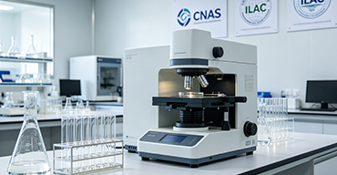
Internationally recognized authority
Certified by multiple international standards such as CNAS, VCS, and GS, with reports universally applicable worldwide.

Global service capability
Covering 140+ countries and regions, it supports on-site detection and remote verification in multiple languages.
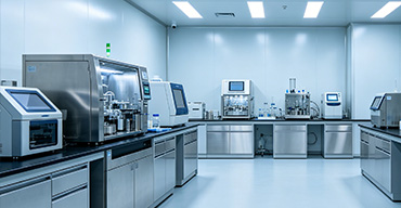
Professional experimental methods
Adopt standard experimental methods to ensure accurate and reliable data.
Deposited Thin Film Coating Testing: Comprehensive Multi-Technique Characterisation for Precision Surfaces
Deposited thin film coatings—ranging from physical vapour deposition (PVD) and chemical vapour deposition (CVD) to atomic layer deposition (ALD) and sol-gel coatings—are ubiquitous in modern technology, serving as protective layers, optical filters, antireflection coatings, barrier films, conductive electrodes, and functional surfaces in microelectronics, optics, aerospace, biomedical devices, and energy systems. The performance of a thin film is not determined solely by its material composition or thickness; it is governed by a complex interplay of microstructure, residual stress, interface adhesion, density, stoichiometry, and surface morphology. Conventional characterisation methods—such as single-wavelength ellipsometry or a simple scratch test—often provide limited information and cannot capture the depth-dependent variations, nanoscale defects, or environmentally induced degradation that critically affect coating lifetime and functionality. Our testing service is specifically designed to deliver a multi-modal, multi-scale, and statistically robust analysis of thin film coatings, covering thickness, optical constants, elemental and chemical states, crystallinity, residual stress, adhesion strength, porosity, and surface roughness. We deploy state-of-the-art laboratory-based and synchrotron-equivalent techniques to resolve features from the atomic level to the macroscopic scale, enabling clients to validate deposition processes, qualify production batches, diagnose field failures, and optimise coating recipes with unprecedented confidence.
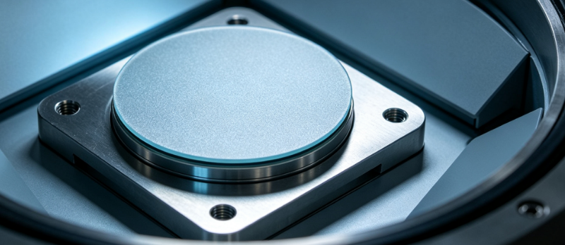
Why Comprehensive Thin Film Testing Is Crucial for Coating Performance and Reliability
Thin films are inherently sensitive to deposition conditions—a 5% variation in chamber pressure, substrate temperature, or deposition rate can alter the film density by several percent, which in turn affects refractive index, hardness, and permeability. Furthermore, the interface between the film and the substrate is often the weakest link; poor adhesion due to contamination, misfit dislocations, or residual stress can lead to delamination under thermal or mechanical load. Standard tests such as a simple tape test or pencil hardness test provide only a pass/fail outcome and offer no quantitative information on the interfacial fracture toughness or the stress gradient across the film. Our testing protocols are designed to fill these gaps, providing a quantitative, physically meaningful characterisation that can be directly correlated with in-service performance—whether the coating is used as a wear-resistant layer on a turbine blade, a dielectric stack in an optical filter, or a diffusion barrier in a semiconductor device. This enables proactive quality control, rapid troubleshooting, and data-driven process improvement.
Our Core Detection Capabilities for Deposited Thin Film Coatings
We operate a fully integrated thin film characterisation platform that combines optical, mechanical, structural, and chemical analysis techniques. The following represent our standard high-end offerings:
Spectroscopic Ellipsometry and Reflectometry (UV–Vis–NIR to MIR): We employ a variable-angle spectroscopic ellipsometer (wavelength range 190–2500 nm, with optional extension to 30 µm) and a spectrophotometer for reflectance/transmittance measurements. We provide film thickness (accuracy ±0.1 nm), optical constants (n, k) over the entire spectral range, and film density (via the Lorentz–Lorenz relation) for single- and multi-layer stacks. Our models incorporate surface roughness and interface grading using effective medium approximations (EMA). We also perform in-situ ellipsometry during deposition or annealing to monitor growth kinetics and phase transitions in real time.
High-Resolution X-Ray Diffraction (HR-XRD) and X-Ray Reflectivity (XRR): Using a high-brightness rotating-anode X-ray source (Cu Kα₁, 18 kW) with a 2D hybrid pixel detector, we perform phase identification, crystallite size determination (via Scherrer analysis), and preferred orientation (texture) analysis. XRR provides film thickness (in the range 1–200 nm) with ±0.1 nm accuracy, surface roughness, and electron density, which is sensitive to porosity. For epitaxial films, we measure lattice mismatch and strain using reciprocal space mapping (RSM).
X-Ray Photoelectron Spectroscopy (XPS) with Depth Profiling: Our monochromatic Al Kα XPS system (spot size 10 µm, energy resolution 0.3 eV) provides quantitative surface chemical composition and chemical state information (oxidation state, bonding environment) with a detection limit of 0.1 at%. We perform angle-resolved XPS (ARXPS) for non-destructive depth profiling (0–10 nm) and Ar⁺ cluster ion sputtering for deeper profiling, allowing us to map composition gradients and interface abruptness (e.g., diffusion of substrate elements into the film). We also detect trace contaminants (e.g., carbon contamination from deposition chamber).
Scanning Electron Microscopy (SEM) and Transmission Electron Microscopy (TEM) with EDX and EELS: Our field-emission SEM (resolution 1 nm) provides topography and cross-sectional imaging for thickness and defect detection. For atomic-scale resolution, we use an aberration-corrected TEM (0.06 nm resolution) with energy-dispersive X-ray spectroscopy (EDX) and electron energy-loss spectroscopy (EELS) for elemental mapping and chemical bonding analysis. We measure grain size distribution, interfacial sharpness, and native oxide layer thickness. We also perform selected area electron diffraction (SAED) for crystallinity.
Nanoindentation and Scratch Testing for Mechanical Properties: A nanoindenter with continuous stiffness measurement (CSM) and a Berkovich tip measures hardness (H) and Young's modulus (E) with a depth resolution of 0.1 nm and a load resolution of 10 nN. We perform depth-profiling hardness to detect substrate influence and creep testing at constant load. Our scratch tester (with acoustic emission monitoring) measures critical load for delamination and provides a quantitative adhesion strength metric (Lc). We also perform micropillar compression on focused ion beam (FIB)-milled pillars for fracture toughness estimation.
Stress Measurement by Wafer Curvature and X-Ray Diffraction: Using a multi-beam optical stress sensor (MOSS) or a laser scanning system, we measure the wafer curvature before and after deposition to derive the average film stress via Stoney's equation (accuracy ±5 MPa). For local stress mapping, we use micro-Raman spectroscopy (peak shift analysis) and sin²ψ XRD to measure residual stress in crystalline films with a lateral resolution of 1 µm. We provide stress-temperature curves by performing measurements at elevated temperatures (up to 500 °C).
Optical, Electrical, and Barrier Property Testing: For functional coatings, we offer four-point probe for sheet resistance (range 10⁻⁶ to 10⁶ Ω/sq), Hall effect for carrier concentration and mobility, impedance spectroscopy for dielectric properties, and water vapour transmission rate (WVTR) and oxygen transmission rate (OTR) measurements for barrier films using a calibrated permeation system (sensitivity down to 10⁻⁶ g/m²/day).
Environmental and Accelerated Ageing Tests: We subject coated samples to temperature cycling (−40 °C to +150 °C), damp heat (85 °C/85% RH), and UV exposure (Xenon arc or UV lamps). We periodically re-measure the film's properties (thickness, stress, adhesion, optical spectra) to evaluate the degradation kinetics. Our accelerated ageing protocol, based on the Arrhenius model, provides a predicted lifetime under realistic service conditions, with typical uncertainty of ±15%.
Advanced Correlative and Modelling Framework
Our unique strength is the integration of multi-technique data into a consistent physical model. We use a proprietary software platform (CoatingSpace™) that aligns the composition profile (from XPS/TEM), the optical dispersion (from ellipsometry), and the mechanical properties (from nanoindentation) to construct a complete property–structure–performance map. For example, we correlate the oxygen vacancy concentration (from XPS) with the refractive index (from ellipsometry) and the residual stress (from XRD), providing a mechanistic explanation for any observed drift. We also perform finite-element simulations (COMSOL or Abaqus) to model the thermal stress distribution in multi-layer stacks, using our measured mechanical properties as inputs. This allows us to predict the critical temperature for delamination or cracking, a service that is invaluable for high-temperature or thermal-cycling applications.
Our Distinctive Advantages in Thin Film Coating Testing
Our laboratory is one of the few commercial facilities that combine all these techniques in one location, with a focus on thin film coatings. We maintain ISO 17025 accreditation for dimensional, optical, and mechanical measurements, and we have a comprehensive database of reference spectra and calibration standards for over 200 coating materials (metals, oxides, nitrides, carbides, polymers, and multilayers). Our team includes surface scientists, optical engineers, and materials physicists with over 25 years of collective experience in thin film characterisation.
We offer flexible sample handling—from small coupons (5 mm × 5 mm) to full 300 mm wafers, and from rigid to flexible substrates. We provide rapid screening (e.g., thickness and optical constants for QC) as well as in-depth research-grade analysis (including HR-TEM and advanced spectroscopy). Our reports are comprehensive and include raw data, processed results, uncertainty budgets, and interpretative commentary. We also offer consulting services to help clients design deposition experiments, select optimal characterisation strategies, and interpret complex data.
Typical turnaround for a standard coating characterisation (thickness, n&k, stress, adhesion, and composition) is 5–7 business days, with a preliminary summary available within 24 hours. For urgent failure analysis, we provide a same-day emergency service for critical samples.
Real-World Impact: Case Highlights from Our Testing
In a recent collaboration with an optics manufacturer, our spectroscopic ellipsometry detected a 1.2 nm interfacial oxide layer between the coating and substrate that was not visible in cross-sectional SEM. This oxide layer reduced adhesion by 30%, causing delamination during thermal cycling. The client adjusted their pre-cleaning process and eliminated the oxide, increasing the coating's lifetime by 200%.
In another project involving a barrier coating for flexible electronics, our WVTR measurements showed that the as-deposited film met the specification, but after 100 hours of damp heat, the permeability increased by a factor of 5. Our XPS depth profiling revealed hydroxyl penetration through pinhole defects. We recommended a densification step (plasma treatment), which reduced the permeability increase to less than 10% after 500 hours.
Partner with Us for Unmatched Coating Characterisation Excellence
Whether you are developing a new protective coating, optimising an optical stack, qualifying a production batch, or investigating a field failure, our detection service delivers the depth, breadth, and precision you need to make informed decisions. We welcome customised test plans—from single-point verification to comprehensive mapping across deposition parameters, substrates, and post-treatment conditions. Our experts are available for collaborative problem-solving and long-term research partnerships.
Let our advanced characterisation unlock the full potential of your thin film coatings. Contact us today to design a testing strategy that meets your most demanding requirements.