Reasons for choosing our testing services
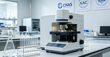
ZHONGXI Testing has obtained inspection qualification certifications from multiple countries and regions worldwide. We possess a senior testing team and advanced testing methods, providing independent, impartial, and professional third-party verification services for global carbon projects.
Internationally recognized authority
Certified by multiple international standards such as CNAS, VCS, and GS, with reports universally applicable worldwide.

Global service capability
Covering 140+ countries and regions, it supports on-site detection and remote verification in multiple languages.

Professional experimental methods
Adopt standard experimental methods to ensure accurate and reliable data.
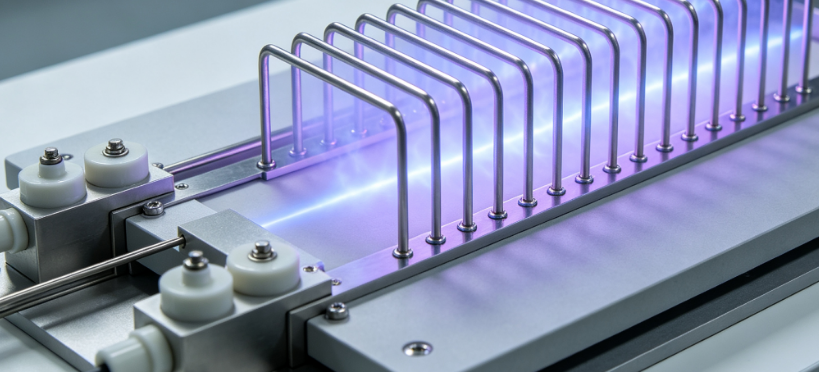
Plasma Barrier Grid Testing: Advanced Structural, Electrical, and Plasma-Interaction Characterisation for High-Integrity Plasma Confinement Systems
Plasma barrier grids—often referred to as plasma fences, ion-optical grids, or dielectric barrier structures—are essential components in a range of advanced technologies, including plasma displays, neutral beam injectors, ion thrusters, plasma etching systems, and fusion edge-localised mode (ELM) control devices. These grids operate under extreme conditions: high electric fields, intense ion/neutral fluxes, thermal cycling, and, in some cases, direct contact with high-density plasma. Their performance hinges not only on precise geometrical tolerances and material purity but also on the electrical integrity of insulating segments, the mechanical stability under thermal stress, the resistance to sputtering, and the suppression of parasitic discharges. Conventional inspection—such as visual checks or simple continuity tests—is grossly insufficient; it cannot detect micro-cracks, dielectric charging, surface contamination, or subtle changes in secondary electron emission that lead to arcing or plasma instability. Our detection service is purpose-built to provide a multi-parameter, non-destructive and destructive characterisation of plasma barrier grids, covering structural geometry, dielectric properties, surface chemistry, high-voltage withstand capability, and plasma-compatibility metrics. We deliver quantitative data on grid aperture uniformity, dielectric breakdown strength, surface charge decay, sputtering yield, and thermal deformation, enabling manufacturers, system integrators, and research laboratories to qualify production batches, validate lifetime models, and diagnose field failures with scientific precision.
Why Dedicated Testing of Plasma Barrier Grids Is Indispensable for Reliable Operation
Plasma barrier grids are typically fabricated from ceramics (alumina, aluminium nitride), glass, or metal-coated dielectrics, with intricate arrays of apertures, ribs, or posts. Their function is to confine or shape the plasma while preventing electrical breakdown between adjacent electrodes. During operation, the grid surface is bombarded by ions and electrons, leading to charge accumulation on dielectric surfaces, which can distort the local electric field and trigger flashover. Furthermore, sputtering of the grid material by high-energy ions gradually erodes the apertures, altering the plasma density profile and reducing the grid's efficiency. Thermal gradients cause differential expansion, which may induce micro-cracking. These degradation mechanisms are often invisible to the naked eye and progress gradually, making early detection essential for predictive maintenance. Our testing protocols are designed to simulate the operational environment and to measure the evolution of critical parameters over time, providing a quantitative basis for life assessment and design improvement.
Our Core Detection Capabilities for Plasma Barrier Grids
We operate a comprehensive test facility that combines precision metrology, electrical characterisation, plasma exposure, and surface analysis. The following represent our standard high-end offerings:
High-Resolution 3D Metrology and Aperture Geometry Analysis: Using a non-contact optical profilometer (vertical resolution 0.1 nm) and a high-resolution X-ray computed tomography (micro-CT) system (voxel size down to 1 µm), we provide complete 3D dimensional maps of the grid, including aperture diameter, rib width, wall angle, and surface roughness (Sa, Sq). We quantify the uniformity of aperture size across the grid (with statistical process control charts) and detect any burrs, chips, or debris that may cause electrical irregularities. For grids with sub-micron features, we use scanning electron microscopy (SEM) with automated image analysis to generate histograms of critical dimensions.
Dielectric Characterisation: Breakdown Strength, Permittivity, and Loss Tangent: We employ a precision LCR meter (20 Hz – 2 MHz) and a dielectric test cell with controlled humidity to measure the relative permittivity (εr) and loss tangent (tan δ) of the grid material, at frequencies relevant to the application (e.g., 13.56 MHz for plasma processing). More importantly, we perform high-voltage dielectric breakdown testing (up to 50 kV DC and 20 kV AC, 50/60 Hz) on representative samples, using a step-stress test or ramp test to determine the Breakdown Voltage and dielectric strength (kV/mm). We also measure the partial discharge inception voltage (PDIV) using a partial discharge detector (sensitivity 1 pC) to identify weak points that may lead to premature failure.
Surface Charge and Secondary Electron Emission Measurements: Using a Kelvin probe and a surface potential metre, we measure the charge decay time constant after exposing the grid to a controlled electron beam or corona discharge. This is critical for predicting the tendency to surface flashover. We also measure the secondary electron yield (SEY) using a dedicated electron gun (0–5 keV) and a hemispherical energy analyser, providing the SEY curve as a function of primary electron energy. This parameter strongly influences plasma stability and multipactor susceptibility.
Plasma Exposure and Sputtering Characterisation: We have a custom-built plasma test chamber (RF or DC) where we can expose the grid (or coupon) to a controlled plasma (argon, oxygen, or other gases) at pressures from 10⁻³ to 10⁰ Pa. During exposure, we monitor ion flux and energy using a retarding field analyser (RFA) and plasma density via a Langmuir probe. After exposure, we perform surface profilometry and SEM/EDS to measure the sputtering rate (nm/hour) and to identify any redeposition of sputtered material. We provide erosion maps across the grid surface, which are correlated with local ion flux distributions to predict lifetime.
Thermal-Mechanical Stability: Thermal Cycling and Warpage Measurement: We subject the grid to programmed thermal cycles (e.g., –40 °C to +300 °C, with controlled ramp rates) using a thermal chamber with optical access. During cycling, we measure out-of-plane warpage using a laser triangulation sensor (resolution 1 µm) and in-plane dimensional changes using a video extensometer. After cycling, we re-measure the aperture dimensions and inspect for cracks using dye penetrant and acoustic emission monitoring during the cycle. This data is used to validate finite-element thermal stress models.
Surface Contamination and Chemical Composition: Using XPS and Auger electron spectroscopy (AES), we analyse the surface chemistry of the grid—detecting any organic contamination, oxidation, or metallic residue from processing. Depth profiling (with Ar⁺ sputtering) reveals the chemical gradient from the surface to the bulk, which is essential for understanding adhesion of subsequent coatings or for identifying source of outgassing.
High-Voltage Impulse and Power Frequency Withstand Testing: We perform lightning impulse tests (1.2/50 µs waveform) and switching impulse tests up to 100 kV, as per IEC and IEEE standards, to qualify grids for high-voltage pulse applications. We also measure the Leakage Current under high DC voltage to assess the surface and volume resistivity of the insulating components.
Integrated Analytical Framework: Correlating Electrical, Mechanical, and Plasma Data
Our unique strength is the synchronised integration of all diagnostic streams. For example, we combine the SEY measurements with the surface roughness data to predict the secondary electron yield reduction factor after plasma exposure. We use the measured sputtering rate and ion flux to compute the effective erosion lifetime and to recommend a safe operating power level. Our proprietary software (GridLife™) automatically imports all the data, applies uncertainty propagation, and generates a comprehensive health score for each grid. This score is composed of sub-indices for geometry, dielectric integrity, surface quality, and thermal resilience, each weighted according to the application's criticality.
We also provide model validation services by comparing our measured results with electromagnetic and thermal simulations (CST, COMSOL). This allows clients to refine their design parameters and to achieve first-pass success in subsequent production runs.
Our Distinctive Advantages in Plasma Barrier Grid Testing
Our laboratory is one of the few facilities equipped with both high-voltage impulse generators and plasma exposure chambers under one roof, enabling seamless sequential testing without sample relocation. We maintain ISO 17025 accreditation for electrical, dimensional, and chemical measurements. Our team includes experienced high-voltage engineers, plasma physicists, and materials scientists with over 20 years of collective expertise in plasma device diagnostics.
We offer tailored test plans—from quick screening of incoming material (thickness, dielectric strength) to comprehensive qualification campaigns involving hundreds of samples and varied environmental conditions. Our reports are detailed and include raw data, statistical analyses, and actionable recommendations. We also provide training and consulting for clients wishing to perform in-house grid testing.
Typical turnaround for a standard characterisation (geometry, dielectric, basic plasma exposure) is 7–10 business days, with a preliminary summary within 48 hours. For urgent failure analysis, we provide a 24-hour priority service.
Real-World Impact: Case Highlights from Our Testing
In a recent evaluation of a plasma display barrier grid, our high-resolution profilometry detected a 3% variation in rib width across the panel, which was not visible to the naked eye. This variation caused non-uniform discharge characteristics, reducing the luminance uniformity by 12%. The manufacturer adjusted their etching process, and the subsequent panels met all uniformity specifications.
In another project involving an ion extraction grid for a fusion neutral beam injector, our plasma exposure tests showed that the molybdenum coating on the grid surface was sputtering at a rate 60% higher than expected, due to a non-optimal ion incidence angle. We recommended a slight tilt of the grid, which reduced the effective sputtering yield by 45%, extending the grid's lifetime by over 2000 hours.
Partner with Us for Unmatched Grid Performance Assurance
Whether you are developing a new plasma barrier grid for a cutting-edge application, qualifying a production batch, or investigating a field failure, our detection service provides the scientific depth, technical precision, and practical insights you need to succeed. We welcome customised test plans—from single-sample verification to full-scale statistical process control studies. Let our advanced diagnostics uncover the hidden vulnerabilities of your grid and guide you towards robust and reliable operation.
Contact us today to design a testing strategy that ensures your plasma barrier grid performs flawlessly under the most demanding conditions.