Reasons for choosing our testing services
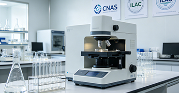
ZHONGXI Testing has obtained inspection qualification certifications from multiple countries and regions worldwide. We possess a senior testing team and advanced testing methods, providing independent, impartial, and professional third-party verification services for global carbon projects.
Internationally recognized authority
Certified by multiple international standards such as CNAS, VCS, and GS, with reports universally applicable worldwide.

Global service capability
Covering 140+ countries and regions, it supports on-site detection and remote verification in multiple languages.

Professional experimental methods
Adopt standard experimental methods to ensure accurate and reliable data.
Comprehensive Gallium Nitride (GaN) Thin-Film Characterization – Advanced Metrology and Quality Assurance Services
Gallium nitride (GaN) and its ternary alloys (InGaN, AlGaN) have become the materials of choice for high‑efficiency light‑emitting diodes, laser diodes, high‑power and high‑frequency transistors, and ultraviolet photodetectors. The performance and reliability of these devices are critically governed by the structural, electrical, optical, and thermal properties of the GaN epitaxial films – from the nucleation layer to the active region and the contact layers. As device architectures evolve toward thinner quantum wells, higher Al compositions, and more complex heterostructures, the demand for multiparametric, spatially resolved, and defect‑sensitive thin‑film characterization has never been greater. Clients seeking GaN thin‑film testing services typically aim to: (i) verify epitaxial quality and crystalline perfection for high‑yield production, (ii) quantify strain, doping, and alloy composition to ensure target device specifications, (iii) detect and classify extended defects (dislocations, stacking faults, pits) that degrade internal quantum efficiency and Leakage Current, (iv) measure thermal conductivity and interface thermal resistance for power device reliability, (v) evaluate surface morphology and contamination levels that affect ohmic contact formation and passivation, and (vi) generate comprehensive qualification data for technology transfer, supplier audits, or regulatory submissions. Our laboratory offers a fully integrated, ISO/IEC 17025‑accredited GaN thin‑film testing service that combines non‑destructive metrology, high‑resolution microscopy, electrical probing, and thermal analysis into a unified assessment platform. We do not simply deliver a list of parameters; we provide correlative structure‑property‑performance models that link deposition conditions (MOCVD, MBE, HVPE) to functional outcomes, enabling our clients to optimize growth, processing, and packaging with scientific rigor and practical efficiency.
Thickness, Composition, and Optical Constants – Spectroscopic Ellipsometry and X‑Ray Reflectivity
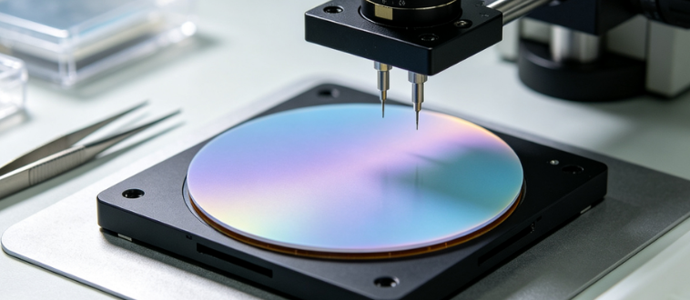
Accurate determination of layer thickness, dielectric function, and alloy composition is fundamental for device design and process control. Our primary non‑destructive tool is a spectroscopic ellipsometer (SE) (J.A. Woollam RC2‑XI) covering 190 nm to 1700 nm with automatic angle scanning (45°–75°) and micro‑spot capability (down to 50 µm). We perform multi‑layer modeling using Tauc‑Lorentz, Cody‑Lorentz, and oscillator models to extract the thickness, refractive index (n), extinction coefficient (k), and roughness of each individual layer (nucleation, buffer, barrier, quantum well, cap) in complex stacks. For AlGaN and InGaN alloys, we determine the bandgap and composition by fitting the dielectric function to standard alloy models, providing Al and In fractions with an accuracy of ±0.005. We combine SE with X‑ray reflectivity (XRR) (PANalytical X'Pert MRD) to independently measure thickness, density, and interface roughness with sub‑nanometer precision, especially valuable for thin (≤20 nm) barrier layers and for assessing the uniformity of ALD‑deposited passivation films.
For the entire wafer, we generate 2D contour maps of thickness, composition, and bandgap with a lateral resolution of 1 mm, revealing radial non‑uniformities that may arise from reactor temperature gradients, gas flow variations, or susceptor aging. Our proprietary fitting algorithm uses a global optimization routine (genetic algorithm plus Levenberg‑Marquardt) to minimize correlation between parameters, delivering robust, physically consistent results even for stacks with up to six absorbing layers. The final report includes full uncertainty budgets and the best‑fit model spectra, ensuring full transparency and traceability.
Crystallinity, Strain, and Phase Purity – High‑Resolution XRD and Reciprocal Space Mapping
The structural quality of GaN thin films is directly reflected in their rocking curve widths, lattice constants, and relaxation state. Our high‑resolution X‑ray diffraction (HR‑XRD) system, equipped with a four‑crystal monochromator and a high‑dynamic‑range detector, performs ω‑2θ scans for symmetric (0002) and asymmetric (10‑12, 20‑21) reflections. The full width at half maximum (FWHM) of the (0002) rocking curve provides a measure of the screw and mixed dislocation density, while the (10‑12) FWHM relates to edge and mixed dislocations, allowing us to estimate the total threading dislocation density (TDD) via the widely accepted mosaic model. Typical values for high‑quality GaN on sapphire or SiC range from 50–300 arcsec for (0002) and 100–600 arcsec for (10‑12). We perform reciprocal space mapping (RSM) around the (10‑15) reflection to evaluate the in‑plane and out‑of‑plane lattice parameters independently, determining the degree of relaxation and the residual biaxial strain. This is particularly critical for thick GaN layers on Si (which often undergo compressive strain) and for AlGaN barrier layers on GaN, where strain affects the piezoelectric polarization and the two‑dimensional electron gas (2DEG) density.
We also provide texture analysis via pole figure measurements to quantify the off‑orientation components and the distribution of crystallographic orientations, which are essential for understanding the nucleation coalescence and the origin of mosaicity. Our XRD reports include a comprehensive analysis of the strain state, the calculated elastic energy, and the predicted bowing of the wafer, enabling clients to fine‑tune the nucleation and buffer conditions for minimal defect density and optimal surface flatness.
Surface Morphology, Roughness, and Defect Inspection – AFM, SEM, and Optical Profilometry
The surface quality of GaN films dictates the interface roughness for subsequent layers, the contact resistance, and the reliability of passivation. We employ atomic force microscopy (AFM) (Bruker Dimension FastScan) in tapping mode to measure surface roughness (Ra, Rq, Rz) over scan areas from 1 µm × 1 µm to 50 µm × 50 µm, providing both statistical parameters and power spectral density (PSD) curves that fingerprint the growth mode (step‑flow, island coalescence, or mound formation). For wide‑area surface inspection, we use a high‑resolution scanning electron microscope (SEM) (FEI Verios 460) equipped with a field‑emission gun and a high‑brightness Schottky emitter, allowing defect detection at resolutions down to 1 nm. Our automated defect classification software (based on deep learning) distinguishes between pits (V‑defects), particles, scratches, and surface delaminations, and provides defect density maps over the entire wafer (up to 200 mm diameter). For high‑throughput, we also employ white‑light interferometry (WLI) and laser confocal microscopy to obtain 3D topography over millimeter‑scale areas, quantifying wafer bow, warp, and global flatness – essential for lithographic alignment and die‑level uniformity.
For buried defects, such as voids or inclusions at the substrate‑film interface, we perform scanning acoustic microscopy (SAM) with a frequency of 100 MHz–1 GHz, detecting subsurface delaminations and porosity with a resolution of 10 µm. The combination of surface and subsurface defect data provides a comprehensive quality index for both epitaxial growth and substrate preparation.
Chemical Composition and Impurity Analysis – XPS, SIMS, and GDMS
The electrical and optical performance of GaN is highly sensitive to impurities (C, O, H, Si, Mg, Fe) and to the stoichiometry (Ga/N ratio). Our surface chemical analysis suite includes X‑ray photoelectron spectroscopy (XPS) with monochromated Al Kα source and in‑situ argon ion sputtering for depth profiling (0–200 nm). We quantify the Ga:N ratio, the amount of native oxide (Ga₂O₃, GaOxNy), and the surface carbon contamination. For bulk impurities, we employ secondary ion mass spectrometry (SIMS) (Cameca IMS 7f) using both O₂⁺ and Cs⁺ primary beams to measure depth profiles of oxygen, carbon, hydrogen, silicon, magnesium, and transition metals with detection limits as low as 1×10¹⁴ atoms/cm³ for O and C. We calibrate with ion‑implanted standards and provide quantitative concentrations versus depth, covering the entire epilayer (up to 10 µm). For total elemental composition, we use glow discharge mass spectrometry (GDMS) on thick (>1 µm) films, offering multi‑element coverage down to sub‑ppm levels.
Furthermore, we perform Rutherford backscattering spectrometry (RBS) (with 2 MeV He⁺) to determine the areal density of Ga and N, providing an independent check on film thickness and stoichiometry without matrix effects. All chemical data are correlated with electrical measurements (Hall, C‑V) to identify the dominant compensation centers, helping clients optimize the growth conditions (e.g., V/III ratio, growth temperature, pressure) to minimize residual impurities.
Electrical Characterization – Hall Effect, C‑V, and Leakage Current Analysis
The electrical properties of GaN films are essential for both transistor and diode applications. We perform room‑temperature and temperature‑dependent Hall effect measurements (van der Pauw geometry) with a magnetic field up to 1.5 T, extracting the sheet resistance, carrier concentration (n or p), and Hall mobility. For temperature‑dependent measurements (77 K to 500 K), we derive the activation energy of donors/acceptors and identify the dominant scattering mechanisms (e.g., phonon, dislocation, impurity). We also fabricate Schottky or MOS capacitors and perform capacitance‑voltage (C‑V) measurements (1 kHz–10 MHz) to extract the depth profile of the carrier concentration, the barrier height, and the interface trap density (Dit). For leakage assessment, we perform I‑V measurements on vertical or lateral diode structures, determining the reverse Breakdown Voltage and the Leakage Current density, which are critical for power device qualification.
For heterostructures (e.g., AlGaN/GaN HEMTs), we measure the 2DEG sheet carrier density and mobility using room‑temperature Hall and temperature‑dependent C‑V, and we correlate these with the strain state (from XRD) and the Al composition (from ellipsometry) to provide a complete picture of the polarization‑induced channel. Our electrical test station (Cascade Summit 11000) with a semiconductor parameter analyzer (Keysight B1500A) is capable of DC, pulsed (10 µs pulse width), and low‑frequency noise measurements, offering deep insights into trapping effects and reliability.
Optical and Photoluminescence Characterization – IQE, Wavelength, and Stability
The optical quality of GaN and its alloys is assessed using photoluminescence (PL) and cathodoluminescence (CL) spectroscopy. Our PL setup includes a 266 nm or 325 nm laser (CW and pulsed), a cryostat (4 K to 300 K), and a high‑resolution spectrograph with a CCD camera. We measure band‑edge emission, near‑bandgap excitonic peaks, and defect‑related yellow luminescence as a function of temperature and excitation power. From the temperature dependence of the integrated PL intensity, we extract the internal quantum efficiency (IQE) by comparing the intensity at 4 K (assuming no non‑radiative recombination) and at 300 K. We also perform time‑resolved PL (TRPL) using a streak camera (resolution < 20 ps) to measure the carrier recombination lifetime, which is directly correlated with the dislocation density and the impurity concentration.
For spatial mapping, we employ CL in a SEM with a parabolic mirror and a photomultiplier tube, acquiring panchromatic and monochromatic images at 5–20 K. This reveals the nanoscale distribution of emission intensity, revealing clusters of non‑radiative defects, V‑defects, and compositional fluctuations in InGaN quantum wells. Our CL system can also acquire hyperspectral maps, providing wavelength‑resolved images that highlight local indium segregation or strain variations. These optical measurements are combined with structural and electrical data to provide a complete quality assessment of the active region.
Thermal Characterization – Conductivity, Resistance, and Reliability
For power electronics and high‑brightness LEDs, thermal management is paramount. We measure the thermal conductivity of GaN thin films using the 3ω method (with frequency‑domain thermoreflectance, FDTR) on patterned test structures, providing in‑plane and cross‑plane conductivities with an accuracy of ±5%. We also perform thermal resistance measurement of packaged devices using the forward‑voltage temperature coefficient (K‑factor) method, extracting the junction temperature and the thermal impedance network. In addition, we conduct accelerated aging tests at high temperature (up to 300 °C) under constant current or constant voltage, with periodic measurement of electrical and optical parameters to determine the activation energy of degradation mechanisms (e.g., contact degradation, defect propagation, or oxidation). Our reliability chamber and thermal cycling system (‑40 °C to +150 °C, up to 2,000 cycles) allow us to simulate field conditions and predict lifetime statistics (Weibull analysis) with high confidence.
Advanced Defect Microscopy – TEM, SEM‑CL, and FIB‑Tomography
For detailed defect analysis, we provide transmission electron microscopy (TEM) (JEOL JEM‑2100F) on cross‑sectional and plan‑view lamellae, with bright‑field, dark‑field, and high‑resolution (HRTEM) imaging. We identify dislocations, stacking faults, micro‑twins, and inversion domains, and we analyze the dislocation density and Burgers vectors using weak‑beam dark‑field. We also perform scanning TEM (STEM) with energy‑dispersive X‑ray spectroscopy (EDS) for elemental mapping at the nanoscale, revealing compositional gradients across interfaces and the distribution of impurities. For 3D information, we use focused ion beam (FIB) tomography to reconstruct the spatial distribution of V‑defects or void networks.
These advanced microscopy techniques are especially valuable for failure analysis and for correlating macroscopic properties (e.g., Leakage Current) with specific microstructural features. Our team includes experienced electron microscopists who can provide detailed interpretations of the observed defects and suggest growth modifications to mitigate them.
Our Distinctive Competencies – Correlative, Quantitative, and Predictive
Our service is distinguished by the correlative integration of all aforementioned techniques on the same set of samples, enabling a holistic understanding of the materials system. We do not simply produce individual numbers; we build structure‑property‑performance databases that allow clients to identify the critical factors limiting their device performance – whether it is a slight strain fluctuation, a subtle carbon incorporation, or a specific dislocation type. Our data science pipeline combines statistical analysis (PCA, PLS) and machine learning to find hidden correlations that are invisible in single‑parameter data sets.
Our scientific team consists of PhDs and engineers with long‑standing expertise in III‑nitride epitaxy, characterization, and device physics. We are active contributors to the GaN community (publications, standards committees) and we understand the practical challenges of MOCVD and MBE growth. We offer consulting services that go beyond reporting – we help you interpret the data, design experiments to test hypotheses, and propose specific changes to growth conditions or device architecture to achieve your performance and reliability targets. We maintain ISO/IEC 17025 accreditation for the majority of our test methods, ensuring full traceability and acceptance by global regulatory bodies and customers.
We offer rapid turnaround times (typically 5‑7 business days for a full characterization suite) and we are flexible in sample size (from a single 5 mm × 5 mm coupon to full 200 mm wafers). Our equipment is maintained at the highest calibration standards, and we participate in international interlaboratory comparisons to ensure our data are consistent with those of other leading facilities.
Comprehensive Service Modules – Tailored to Your Application
We offer a modular testing structure that allows you to select the exact measurements needed for your specific GaN film:
Module 1 – Physical Thickness and Optical Constants: Spectroscopic ellipsometry (n,k, thickness) and XRR (density, roughness) – essential for layer design verification.
Module 2 – Crystallinity and Strain State: HR‑XRD rocking curves, RSM, and texture analysis – critical for dislocation density and stress assessment.
Module 3 – Surface and Defect Inspection: AFM (roughness), SEM (defect classification), WLI (flatness), and SAM (subsurface) – for surface quality and yield prediction.
Module 4 – Chemical and Impurity Profiling: XPS (stoichiometry, oxide), SIMS (dopants, C, O, H), RBS (areal density) – for purity and doping control.
Module 5 – Electrical Transport and C‑V: Hall (mobility, carrier concentration), C‑V (depth profile, Dit), and I‑V (leakage, breakdown) – for device modeling and reliability.
Module 6 – Optical and Luminescence Characterization: PL (IQE, wavelength), TRPL (lifetime), CL (spatial maps, defect bands) – for active region quality and efficiency.
Module 7 – Thermal and Reliability Testing: Thermal conductivity (3ω), thermal resistance (K‑factor), and accelerated aging (high‑temp/current stress) – for lifetime prediction and packaging optimization.
Module 8 – Comprehensive GaN Film Qualification Package: All modules combined, plus a final integrated report with correlations, statistical analysis, and expert recommendations – suitable for technology qualification, supplier auditing, or regulatory submission.
We can also design custom test plans for non‑standard structures (e.g., ultra‑thin barriers, graded layers, or novel alloys like ScAlN).
Data Integrity, Security, and Client Engagement
All measurements are performed under strictly controlled conditions (class 100 cleanroom for sensitive samples), with NIST‑traceable calibrations and comprehensive SOPs. Our data management system records every operation, operator, and environmental parameter, providing full audit trails. We adhere to strict confidentiality protocols – all client data are encrypted, access‑controlled, and retained securely. We provide comprehensive reports with tables, graphs, uncertainty statements, and an executive summary that translates the technical findings into business‑relevant insights. We also offer post‑report consultation via teleconference to review the results and discuss their implications for your project.
Engaging our service is straightforward: we start with a free consultation to understand your sample and goals, then provide a detailed proposal with pricing and timeline. Upon sample receipt, we log, inspect, and begin analysis, with regular updates via our client portal. The final report is delivered in PDF with editable data files upon request.
Conclusion – Empowering Your GaN Technology with Unmatched Analytical Depth
Gallium nitride thin‑film technology is advancing at a rapid pace, but success in both R&D and production depends on the ability to measure, understand, and control the material’s structural, chemical, electrical, optical, and thermal properties with high precision and in a correlated manner. Our comprehensive testing service provides exactly that – a one‑stop, ISO‑accredited, and scientifically rigorous solution that transforms measurement data into actionable intelligence. With our advanced instrumentation, deep materials expertise, and collaborative approach, we empower our clients to accelerate development, reduce cycle times, and achieve the reliability and performance required for competitive products.
We invite you to contact our GaN characterization specialists to discuss your specific thin‑film testing requirements. Let us partner with you to ensure that your GaN epiwafers and devices meet the highest standards of quality and performance – from the buffer layer to the final device. Your journey to GaN excellence begins with our expert testing and insightful analysis.