Reasons for choosing our testing services
ZHONGXI Testing has obtained inspection qualification certifications from multiple countries and regions worldwide. We possess a senior testing team and advanced testing methods, providing independent, impartial, and professional third-party verification services for global carbon projects.
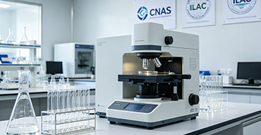
Internationally recognized authority
Certified by multiple international standards such as CNAS, VCS, and GS, with reports universally applicable worldwide.

Global service capability
Covering 140+ countries and regions, it supports on-site detection and remote verification in multiple languages.

Professional experimental methods
Adopt standard experimental methods to ensure accurate and reliable data.
Comprehensive Nitride Semiconductor Wafer Inspection and Characterization – Advanced Analytical Services
Nitride semiconductor wafers – encompassing gallium nitride (GaN), aluminum nitride (AlN), indium nitride (InN), and their ternary and quaternary alloys – form the material foundation for a new generation of high‑power, high‑frequency, and deep‑ultraviolet optoelectronic devices. Whether used as free‑standing substrates, as epitaxial layers on foreign substrates (sapphire, silicon carbide, silicon), or as engineered templates, the quality of these wafers directly determines device efficiency, reliability, and manufacturing yield. Clients seeking nitride semiconductor wafer testing services typically aim to: (i) qualify incoming wafers and monitor batch‑to‑batch consistency, (ii) detect crystallographic defects, surface imperfections, and subsurface damage that propagate into device failures, (iii) verify electrical properties such as carrier concentration, mobility, and sheet resistance, (iv) assess optical quality including bandgap, transmittance, and luminescence efficiency, (v) profile dopants and impurities that affect conductivity and reliability, and (vi) generate comprehensive material certificates for process integration, customer audits, and regulatory submissions. Our laboratory offers a fully integrated, ISO/IEC 17025‑accredited nitride semiconductor wafer testing service that combines high‑resolution X‑ray diffraction, advanced electron microscopy, spectroscopic ellipsometry, secondary ion mass spectrometry, Hall effect, photoluminescence, atomic force microscopy, and non‑contact electrical metrology into a unified assessment platform. We do not merely report pass/fail results; we deliver a holistic wafer quality fingerprint that correlates crystal growth, epitaxial parameters, and wafer processing with device‑level performance, empowering our clients to accelerate development, reduce defects, and achieve global market access with confidence.
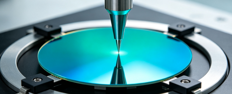
Why Professional Nitride Wafer Testing Is Indispensable for Device Yield and Reliability
Nitride semiconductors are notoriously sensitive to crystalline imperfections. Threading dislocations, stacking faults, inversion domains, and basal plane defects act as non‑radiative recombination centers, leakage paths, and reliability killers. Even a slight deviation in alloy composition or doping can shift the emission wavelength, degrade carrier mobility, or cause premature breakdown. In power electronics, wafer‑level defects such as micropipes, voids, and surface pits can lead to catastrophic failure under high voltage. In RF devices, trap‑related effects cause current collapse and dynamic on‑resistance. For deep‑UV emitters, aluminum composition uniformity and oxygen contamination directly impact internal quantum efficiency. Without rigorous wafer‑level characterization, these issues remain hidden until device fabrication, resulting in costly yield loss and delayed time‑to‑market. Our testing services provide the objective evidence needed to diagnose process drift, qualify new suppliers, and support technology transfer. We help clients navigate the complex landscape of standards and specifications, including SEMI M1, M55, M67, ASTM F1188, and ISO 14707, ensuring that every nitride wafer meets the stringent requirements of its intended application.
Our Comprehensive Wafer Characterization Platform – From Crystal Quality to Electrical Properties
We evaluate nitride semiconductor wafers across the entire lifecycle, from as‑grown ingots and sliced substrates to fully processed epitaxial wafers. Our capabilities include:
Crystalline Perfection and Defect Analysis: High‑resolution X‑ray diffraction (HR‑XRD) with a four‑crystal monochromator and triple‑axis analyzer measures rocking curve widths (FWHM) for symmetric and asymmetric reflections, providing quantitative dislocation densities. Reciprocal space mapping (RSM) separates strain and composition effects. Transmission electron microscopy (TEM) with aberration correction reveals atomic‑scale defect structures, while cathodoluminescence (CL) mapping locates non‑radiative recombination centers with high spatial resolution. Raman spectroscopy quantifies stress and crystalline quality, and etch pit density (EPD) measurements provide statistical defect counts over large areas.
Surface Morphology and Defect Inspection: Atomic force microscopy (AFM) measures surface roughness (Ra, Rq, Rz) and step‑flow morphology with sub‑nanometer resolution. Field‑emission scanning electron microscopy (FE‑SEM) with automated defect classification identifies pits, particles, scratches, and cracks. White‑light interferometry (WLI) and laser confocal microscopy provide 3D topography and wafer flatness data. Scanning acoustic microscopy (SAM) detects subsurface delamination and voids in bonded or laminated wafers.
Electrical Properties: Room‑temperature and temperature‑dependent Hall effect measurements (van der Pauw) determine sheet resistance, carrier concentration, and mobility. Capacitance‑voltage (C‑V) profiling extracts carrier depth profiles and interface trap densities. Non‑contact resistivity and sheet resistance mapping (eddy current, four‑point probe) provide rapid, non‑destructive uniformity assessment. For HEMT structures, we measure two‑dimensional electron gas (2DEG) density and mobility, correlating with strain and alloy composition.
Optical Properties: UV‑Vis‑NIR spectrophotometry with an integrating sphere measures transmittance, reflectance, and absorption. Spectroscopic ellipsometry determines thickness, refractive index (n), and extinction coefficient (k) of individual layers, as well as alloy composition and bandgap. Photoluminescence (PL) at room and cryogenic temperatures (4 K) reveals excitonic transitions, defect‑related emission, and internal quantum efficiency (IQE). Time‑resolved PL (TRPL) measures carrier lifetimes, while cathodoluminescence (CL) mapping visualizes spatial variations in emission.
Composition, Doping, and Impurity Profiling: Secondary ion mass spectrometry (SIMS) with O₂⁺ and Cs⁺ primary beams provides depth profiles of dopants (Si, Mg, C, O, H) and impurities with detection limits down to 1×10¹⁵ atoms/cm³. X‑ray photoelectron spectroscopy (XPS) quantifies surface stoichiometry, native oxide thickness, and chemical states. Rutherford backscattering spectrometry (RBS) provides areal density and depth profiles without matrix effects. Auger electron spectroscopy (AES) offers high‑spatial‑resolution chemical mapping of interfaces.
Stress, Curvature, and Thermal Properties: Wafer curvature and bow measurements using laser scanning or interferometry quantify residual stress and its uniformity. Raman spectroscopy provides local stress mapping with sub‑micron resolution. Thermal conductivity is measured by the 3ω method or frequency‑domain thermoreflectance (FDTR), and thermal resistance of packaged devices is determined by the forward‑voltage temperature coefficient (K‑factor) method.
Wafer Geometry and Flatness: Non‑contact thickness gauges and interferometers measure total thickness variation (TTV), bow, warp, and site flatness (SFQR) according to SEMI standards. We provide full‑wafer contour maps with 1 mm resolution, enabling identification of radial non‑uniformities from slicing, lapping, polishing, or epitaxial growth.
Advanced Failure Analysis and Root‑Cause Diagnostics
When wafers fail to meet specifications or exhibit unexpected degradation, our failure analysis (FA) service provides a systematic, multi‑technique investigation. Our FA workflow includes:
(i) Optical and confocal microscopy for visual inspection of surface damage, discoloration, and macro‑defects.
(ii) Scanning electron microscopy (SEM) with EDS for high‑magnification imaging and elemental analysis of defects, contamination, and etch pits.
(iii) Focused ion beam (FIB) cross‑sectioning combined with TEM and SAED to examine dislocation cores, stacking faults, and interface structures at the atomic scale.
(iv) Atom probe tomography (APT) for 3D atom‑by‑atom reconstruction of dopant clusters, segregation, and interfacial chemistry.
(v) Electron‑beam‑induced current (EBIC) and cathodoluminescence (CL) mapping to locate recombination centers and correlate them with structural defects.
We integrate all FA data with the wafer’s growth and processing history to construct a complete failure timeline, attributing the root cause to specific growth parameters, substrate quality, or handling procedures. This level of diagnostic depth is rarely available in commercial test houses and is highly valued by clients involved in yield improvement, supplier qualification, and technology transfer.
Our Distinctive Competencies – Integration, Expertise, and Global Compliance
What sets our nitride semiconductor wafer testing service apart is the seamless integration of structural, electrical, optical, chemical, and morphological characterization within a single laboratory, enabling correlative analysis that is impossible when samples are shipped between multiple vendors. Our team comprises PhD‑level materials scientists, physicists, and engineers with extensive experience in III‑nitride epitaxy, wafer processing, and device physics. We do not simply report numbers; we interpret them in terms of growth chemistry, defect kinetics, and device performance – for example, distinguishing between strain‑induced and composition‑induced changes in bandgap, or identifying whether a mobility reduction arises from interface roughness scattering or impurity compensation.
Our laboratory is ISO/IEC 17025 accredited for many of the key test methods (XRD, SIMS, Hall, PL, AFM, XPS), and we maintain NIST‑traceable calibrations for all equipment. We participate in international round‑robins (e.g., VAMAS, ASTM, SEMI) to ensure global comparability. We offer rapid turnaround – typically 3–5 business days for a standard characterization package – and we accept samples in various forms: full wafers (up to 200 mm), diced coupons, and small pieces. Our data analytics platform employs machine learning to identify subtle correlations between growth parameters and wafer properties, accelerating process optimization.
We also provide custom test plans for emerging nitride materials (e.g., AlN, ScAlN, BAlN) and for non‑standard wafer architectures (e.g., engineered substrates, patterned sapphire, free‑standing GaN). Our consulting services include interpretation of results, design of experiments (DoE) for process improvement, and troubleshooting of epitaxial defects. We offer on‑site sampling and mobile testing units for large‑scale wafer fabs, ensuring that critical measurements can be performed without transport delays.
Comprehensive Service Modules – Tailored to Your Wafer Type and Stage
We offer a modular testing structure that allows clients to select the exact measurements needed for their specific nitride wafer:
Module 1 – Crystal Quality and Defect Analysis: HR‑XRD, TEM, Raman, CL, and EPD – essential for substrate and epitaxial quality control.
Module 2 – Surface and Subsurface Inspection: AFM, SEM, WLI, SAM, and laser confocal microscopy – for morphology, flatness, and subsurface defects.
Module 3 – Electrical Properties: Hall effect, C‑V, non‑contact resistivity, and 2DEG characterization – for carrier concentration, mobility, and sheet resistance.
Module 4 – Optical Properties: Transmittance, ellipsometry, PL, TRPL, and CL mapping – for bandgap, thickness, and luminescence efficiency.
Module 5 – Composition, Doping, and Impurity Profiling: SIMS, XPS, RBS, and AES – for stoichiometry, dopant depth profiles, and interface chemistry.
Module 6 – Stress, Curvature, and Thermal Analysis: Wafer curvature, Raman stress mapping, thermal conductivity (3ω), and junction temperature measurement – for thermal management and reliability.
Module 7 – Comprehensive Wafer Qualification Package: All modules combined into a single project, with integrated analysis, statistical summary, and a detailed interpretive report – suitable for technology transfer, supplier qualification, or regulatory submission.
We also design custom test plans for special requirements, such as high‑resolution XRD for ultrathin layers, temperature‑dependent Hall up to 500 K, or polarization‑resolved PL.
Data Integrity, Security, and Reporting
All measurements are performed under strictly controlled conditions (class 100 cleanroom for sensitive samples), with NIST‑traceable calibrations and comprehensive SOPs. Our Laboratory Information Management System (LIMS) records every operation, operator, and environmental parameter, ensuring full auditability. We adhere to strict confidentiality protocols – all client data are encrypted, access‑controlled, and retained securely. We provide comprehensive reports with tables, graphs, uncertainty statements, and an executive summary that translates technical findings into actionable business insights. Raw data files are available upon request. A post‑delivery review meeting is included to discuss results and recommend next steps.
Client Engagement and Workflow
Our engagement begins with a complimentary consultation to understand your wafer type (GaN, AlN, InN, AlGaN, InGaN), deposition method, intended device application, and specific concerns (e.g., dislocation density, doping uniformity, or surface roughness). We then propose a tailored test plan with a fixed price and timeline. Upon sample receipt, we log and inspect the samples, then commence testing. Clients receive progressive updates through a secure portal, with preliminary data shared on request. The final report is delivered in PDF format, and we offer a follow‑up call to discuss the findings and their implications for your development or production.
Conclusion – Ensuring Nitride Wafer Excellence from Substrate to Device
Nitride semiconductor wafers are the foundation of modern high‑performance optoelectronics and power electronics, and their precise characterization is essential for achieving competitive yield, reliability, and performance. Our comprehensive, ISO‑accredited testing service provides exactly that – a one‑stop solution that combines structural, electrical, optical, chemical, and morphological analyses into a unified, interpretable picture. With our advanced instrumentation, deep materials expertise, and collaborative approach, we empower our clients to accelerate development, reduce defects, and confidently bring high‑quality nitride devices to market.
We invite you to contact our nitride wafer characterization specialists to discuss your specific testing needs. Let us partner with you to ensure that your nitride wafers meet the highest standards of quality and performance – from the crystal growth furnace to the final device. Your journey to nitride wafer excellence begins with our rigorous, integrative, and actionable testing.