Reasons for choosing our testing services
ZHONGXI Testing has obtained inspection qualification certifications from multiple countries and regions worldwide. We possess a senior testing team and advanced testing methods, providing independent, impartial, and professional third-party verification services for global carbon projects.
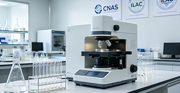
Internationally recognized authority
Certified by multiple international standards such as CNAS, VCS, and GS, with reports universally applicable worldwide.

Global service capability
Covering 140+ countries and regions, it supports on-site detection and remote verification in multiple languages.

Professional experimental methods
Adopt standard experimental methods to ensure accurate and reliable data.
Advanced Gallium Nitride (GaN) Substrate Inspection and Characterization Services – Ensuring Epitaxial Excellence
Gallium nitride (GaN) substrates – particularly free‑standing GaN wafers – are the ultimate foundation for high‑performance optoelectronic and electronic devices, including laser diodes, high‑electron‑mobility transistors (HEMTs), and ultraviolet photodetectors. Unlike heteroepitaxial growth on foreign substrates, homoepitaxy on GaN substrates dramatically reduces threading dislocation density, enabling superior device efficiency, reliability, and lifetime. However, the quality of the GaN substrate itself – its crystalline perfection, surface finish, impurity content, and electrical uniformity – directly dictates the outcome of subsequent epitaxial growth and device fabrication. Clients seeking GaN substrate testing services typically aim to: (i) qualify incoming substrates from suppliers, (ii) verify dislocation density and crystal quality before committing to expensive epitaxy, (iii) assess surface roughness and subsurface damage that could propagate into the active region, (iv) measure electrical properties for conductive or semi‑insulating substrates, and (v) obtain comprehensive material certificates for process integration, customer audits, and technology transfer. Our laboratory offers a fully integrated, ISO/IEC 17025‑accredited GaN substrate characterization service that combines high‑resolution X‑ray diffraction, transmission electron microscopy, atomic force microscopy, Raman spectroscopy, Hall effect, secondary ion mass spectrometry, photoluminescence, and non‑contact metrology into a unified assessment platform. We do not merely report parameters; we deliver a holistic substrate quality fingerprint that correlates crystal growth, wafer processing, and surface preparation with epitaxial readiness, empowering our clients to accelerate development, reduce defects, and achieve competitive advantage in the GaN device market.
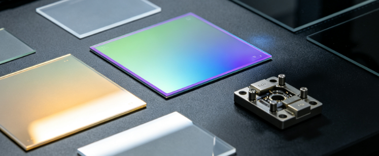
Why Professional GaN Substrate Testing Is Indispensable for Device Yield and Reliability
GaN substrates are expensive and often produced in limited quantities. A substrate with hidden defects – such as a high density of threading dislocations, basal plane stacking faults, or subsurface polishing damage – can ruin an entire epitaxial run, wasting time, precursors, and money. Moreover, the performance of GaN‑based lasers and power devices is extremely sensitive to substrate quality: dislocations act as non‑radiative recombination centers and leakage paths; residual strain causes wafer bow and wavelength non‑uniformity; impurities like oxygen and carbon compensate dopants and increase optical loss. Regulatory and industry standards such as SEMI M1, M55, M67, ASTM F1188, and ISO 14707 impose strict requirements on testing methods and data reporting. Our testing services provide the objective evidence needed to diagnose process drift, qualify new suppliers, and support technology transfer. We help clients navigate the complex landscape of standards, ensuring that every GaN substrate meets the stringent requirements of its intended application and regulatory jurisdiction.
Comprehensive Crystal Quality and Defect Analysis – XRD, TEM, Raman, and X‑ray Topography
The crystalline perfection of GaN substrates is the primary determinant of epitaxial layer quality. Our primary technique is high‑resolution X‑ray diffraction (HR‑XRD) (PANalytical X'Pert MRD) with a four‑crystal monochromator and a triple‑axis analyzer. We perform ω‑2θ scans on symmetric (0002) and asymmetric (10‑12) reflections to determine lattice parameters, strain state, and crystallite size. Rocking curve (ω‑scan) measurements provide the full width at half maximum (FWHM), which is directly correlated with screw and edge dislocation densities. Typical high‑quality GaN substrates exhibit FWHM values below 50 arcsec for (0002) and below 150 arcsec for (10‑12). We also perform reciprocal space mapping (RSM) to separate in‑plane and out‑of‑plane lattice parameters, revealing any residual strain or relaxation gradients. For nanoscale defect analysis, we use transmission electron microscopy (TEM) (JEOL JEM‑2100F) on cross‑sectional lamellae prepared by focused ion beam (FIB). High‑resolution TEM (HRTEM) reveals atomic‑scale dislocation cores, stacking faults, and inversion domains. Scanning TEM (STEM) with energy‑dispersive X‑ray spectroscopy (EDS) provides 2D elemental mapping to detect impurity segregation at defects. We complement XRD and TEM with Raman spectroscopy (Horiba LabRAM HR Evolution) using a 532 nm laser to measure the E₂(high) phonon mode, which is sensitive to residual stress and crystalline quality. X‑ray topography (Lang method) provides large‑area, non‑destructive mapping of dislocation distributions and long‑range strain fields, enabling visualization of slip bands, micropipes, and growth striations. We also perform etch pit density (EPD) measurements using molten KOH or H₃PO₄ etching, followed by automated optical microscopy counting, to provide a statistical measure of dislocation density over the entire wafer.
Surface Morphology, Flatness, and Subsurface Damage Assessment
The surface finish of a GaN substrate influences nucleation, step‑flow growth, and interface abruptness during homoepitaxy. Our surface metrology suite includes atomic force microscopy (AFM) (Bruker Dimension FastScan) in tapping mode to measure surface roughness (Ra, Rq, Rz) over scan areas from 1 μm × 1 μm to 50 μm × 50 μm. We provide statistical parameters and power spectral density (PSD) curves that fingerprint the polishing quality and reveal scratches, pits, or surface steps. For wide‑area inspection, we use a field‑emission scanning electron microscope (FE‑SEM) (FEI Verios 460) with automated defect classification, enabling detection of particles, cracks, and delamination. White‑light interferometry (WLI) and laser confocal microscopy provide 3D topography over millimeter‑scale areas, quantifying wafer bow, warp, and global flatness (TTV, SFQR) according to SEMI standards. Subsurface damage – the residual damaged layer from sawing, grinding, and chemical‑mechanical polishing – is assessed using confocal Raman depth profiling with 2 nm step size and cross‑sectional TEM. We measure the thickness of the damaged layer and its crystalline quality, providing actionable data for optimizing CMP and etching processes. For buried defects such as voids or inclusions, we use scanning acoustic microscopy (SAM) with a frequency of 100 MHz–1 GHz, achieving a spatial resolution of 10 μm.
Electrical and Optical Properties – Hall Effect, C‑V, PL, and CL
For conductive or semi‑insulating GaN substrates, electrical properties are critical for device design. We perform room‑temperature and temperature‑dependent Hall effect measurements (van der Pauw geometry) with a magnetic field up to 1.5 T, extracting sheet resistance, carrier concentration (n‑type or p‑type), and Hall mobility. For high‑resistivity substrates, we use a high‑impedance electrometer and guard‑ring configurations to minimize leakage. We also perform capacitance‑voltage (C‑V) measurements on Schottky or MIS structures to determine the built‑in potential, depletion width, and interface trap density (Dit). For doping profiling, we use electrochemical capacitance‑voltage (ECV) profiling, which provides depth‑resolved carrier concentration without destructive sample preparation. Optical quality is assessed using photoluminescence (PL) spectroscopy at room temperature and 4 K using a 325 nm HeCd laser. The near‑band‑edge emission and deep‑level emission bands reveal excitonic transitions, impurity‑related defects, and non‑radiative recombination centers. Time‑resolved PL (TRPL) with a streak camera (resolution < 20 ps) measures carrier lifetime, which correlates with dislocation density and impurity concentration. We also perform cathodoluminescence (CL) mapping in a SEM at 5–20 K to visualize spatial variations in emission at the microscale, revealing dark spots corresponding to individual dislocations or defect clusters.
Impurity and Dopant Profiling – SIMS, GDMS, XPS, and ICP‑MS
Trace impurities in GaN substrates can severely degrade device performance. Oxygen and carbon are common unintentional dopants that compensate intentional dopants and increase optical loss. Our secondary ion mass spectrometry (SIMS) (Cameca IMS 7f) using both O₂⁺ and Cs⁺ primary beams provides depth profiles of O, C, Si, H, Mg, and transition metals with detection limits as low as 1×10¹⁵ atoms/cm³ for O and C and 1×10¹⁴ atoms/cm³ for transition metals. We calibrate with ion‑implanted standards, ensuring quantitative accuracy across the entire substrate thickness. For bulk trace element analysis, we use glow discharge mass spectrometry (GDMS), which covers over 70 elements with detection limits down to 0.01 ppb. X‑ray photoelectron spectroscopy (XPS) with in‑situ ion sputtering quantifies surface stoichiometry, native oxide thickness, and chemical states (e.g., Ga‑O, Ga‑N, C‑N). Inductively coupled plasma mass spectrometry (ICP‑MS) provides complementary bulk analysis for metals. All chemical data are correlated with electrical and optical measurements to identify compensation mechanisms and to guide substrate selection or pre‑growth cleaning optimization.
Thermal and Mechanical Characterization – Thermal Conductivity, CTE, and Curvature
Thermal management is critical for high‑power GaN devices, and the substrate’s thermal properties directly affect junction temperature and reliability. We measure the thermal conductivity of GaN substrates using the 3ω method or frequency‑domain thermoreflectance (FDTR) on patterned test structures, providing in‑plane and cross‑plane conductivities with ±5% accuracy. We also measure the coefficient of thermal expansion (CTE) using a push‑rod dilatometer from room temperature to 1000 °C, with an accuracy of ±0.02 ppm/K. Wafer curvature and bow are measured using a laser scanning system with a spatial resolution of 1 mm, and the residual stress is calculated using Stoney’s equation. We also perform thermal cycling (−40 °C to +150 °C, up to 2,000 cycles) to evaluate the thermal‑mechanical stability of the substrate and any associated coatings or bonding layers. Mechanical properties such as hardness and fracture toughness are measured using a nanoindenter (Berkovich tip) and four‑point bending tests, providing data essential for wafer handling, dicing, and thinning processes.
Our Distinctive Competencies – Accreditation, Expertise, Integration, and Rapid Turnaround
What sets our GaN substrate testing service apart is the seamless integration of structural, electrical, optical, chemical, and thermal characterization within a single laboratory, enabling correlative analysis that is impossible when samples are shipped between multiple vendors. Our team comprises PhD‑level materials scientists, physicists, and engineers with extensive experience in III‑nitride crystal growth, wafer processing, and device physics. We do not simply report numbers; we interpret them in terms of growth chemistry, defect kinetics, and epitaxial readiness – for example, distinguishing between dislocations that are benign and those that will act as killer defects in a laser diode, or identifying the root cause of surface roughness as polishing damage versus contamination.
Our laboratory is ISO/IEC 17025 accredited for many of the key test methods (XRD, SIMS, Hall, PL, AFM, XPS), and we maintain NIST‑traceable calibrations for all equipment. We participate in international round‑robins (e.g., VAMAS, ASTM, SEMI) to ensure global comparability. We offer rapid turnaround – typically 3–5 business days for a standard characterization package – and we accept samples in various forms: full wafers (up to 200 mm), diced coupons, and small pieces. Our data analytics platform employs machine learning to identify subtle correlations between growth parameters and substrate properties, accelerating process optimization.
We also provide custom test plans for emerging GaN substrate technologies (e.g., ammonothermal GaN, Na‑flux GaN, and engineered substrates) and for non‑standard device architectures (e.g., vertical GaN power devices, micro‑LEDs). Our consulting services include interpretation of results, design of experiments (DoE) for process improvement, and troubleshooting of epitaxial defects. We offer on‑site sampling and mobile testing units for large‑scale wafer fabs, ensuring that critical measurements can be performed without transport delays.
Comprehensive Service Modules – Tailored to Your Substrate Specifications
We offer a modular testing structure that allows clients to select the exact measurements needed for their specific GaN substrate:
Module 1 – Crystal Quality and Defect Analysis: HR‑XRD, TEM, Raman, X‑ray topography, and EPD – essential for substrate qualification and supplier comparison.
Module 2 – Surface and Subsurface Inspection: AFM, SEM, WLI, SAM, and Raman depth profiling – for roughness, flatness, and subsurface damage.
Module 3 – Electrical Properties: Hall effect, C‑V, ECV, and non‑contact resistivity – for carrier concentration, mobility, and doping uniformity.
Module 4 – Optical Properties: PL, TRPL, and CL mapping – for band edge quality, defect emission, and spatial homogeneity.
Module 5 – Impurity and Dopant Profiling: SIMS, GDMS, XPS, and ICP‑MS – for trace impurities, dopant depth profiles, and surface chemistry.
Module 6 – Thermal and Mechanical Properties: Thermal conductivity (3ω), CTE, wafer curvature, nanoindentation, and four‑point bending – for thermal management and handling reliability.
Module 7 – Comprehensive GaN Substrate Qualification Package: All modules combined, plus a final integrated report with correlations, statistical analysis, and expert recommendations – suitable for technology transfer, supplier qualification, or regulatory submission.
We also design custom test plans for special requirements, such as high‑resolution XRD for ultrathin layers, temperature‑dependent Hall up to 500 K, or polarization‑resolved PL.
Data Integrity, Security, and Reporting
All measurements are performed under strictly controlled conditions (class 100 cleanroom for sensitive samples), with NIST‑traceable calibrations and comprehensive SOPs. Our Laboratory Information Management System (LIMS) records every operation, operator, and environmental parameter, ensuring full auditability. We adhere to strict confidentiality protocols – all client data are encrypted, access‑controlled, and retained securely. We provide comprehensive reports with tables, graphs, uncertainty statements, and an executive summary that translates technical findings into actionable business insights. Raw data files are available upon request. A post‑delivery review meeting is included to discuss results and recommend next steps.
Client Engagement and Workflow
Our engagement begins with a complimentary consultation to understand your GaN substrate type (free‑standing, template, or engineered), intended device application, and specific concerns (e.g., dislocation density, surface roughness, or doping uniformity). We then propose a tailored test plan with a fixed price and timeline. Upon sample receipt, we log and inspect the samples, then commence testing. Clients receive progressive updates through a secure portal, with preliminary data shared on request. The final report is delivered in PDF format, and we offer a follow‑up call to discuss the findings and their implications for your development or production.
Conclusion – Ensuring GaN Substrate Excellence from Crystal to Device
Gallium nitride substrates are the cornerstone of high‑performance optoelectronics and power electronics, and their precise characterization is essential for achieving competitive yield, reliability, and performance. Our comprehensive, ISO‑accredited testing service provides exactly that – a one‑stop solution that combines structural, electrical, optical, chemical, and thermal analyses into a unified, interpretable picture. With our advanced instrumentation, deep materials expertise, and collaborative approach, we empower our clients to accelerate development, reduce defects, and confidently bring high‑quality GaN‑based devices to market.
We invite you to contact our GaN substrate characterization specialists to discuss your specific testing needs. Let us partner with you to ensure that your GaN substrates meet the highest standards of quality and performance – from the crystal growth furnace to the final device. Your journey to GaN substrate excellence begins with our rigorous, integrative, and actionable testing.