Reasons for choosing our testing services
ZHONGXI Testing has obtained inspection qualification certifications from multiple countries and regions worldwide. We possess a senior testing team and advanced testing methods, providing independent, impartial, and professional third-party verification services for global carbon projects.
Internationally recognized authority
Certified by multiple international standards such as CNAS, VCS, and GS, with reports universally applicable worldwide.

Global service capability
Covering 140+ countries and regions, it supports on-site detection and remote verification in multiple languages.

Professional experimental methods
Adopt standard experimental methods to ensure accurate and reliable data.
Precision Silicon Oxynitride (SiON) Analysis – Uncovering Composition, Structure, and Performance at the Atomic Level
When you search for silicon oxynitride (SiON) detection, you are likely preparing to qualify this critical material for advanced applications – whether in semiconductor gate dielectrics, passivation layers, anti-reflective coatings, optoelectronic waveguides, high-temperature structural ceramics, or biomedical barriers. Silicon oxynitride offers a tunable balance between silicon dioxide (SiO₂) and silicon nitride (Si₃N₄), giving you unique control over refractive index, dielectric constant, mechanical strength, oxidation resistance, and interfacial stress. However, these performance advantages are only as reliable as your ability to measure the exact oxygen-to-nitrogen ratio, hydrogen impurities, bond configuration, film density, and defect states. Our detection service is engineered to deliver that clarity – with precision and depth unmatched in the industry.
Our Silicon Oxynitride Characterisation Capabilities – What We Measure and How Deep We Go
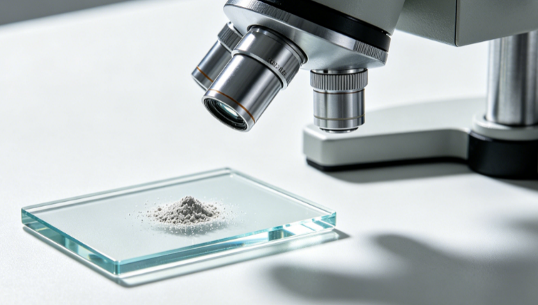
We deploy an integrated suite of advanced analytical techniques that together provide a complete, multi-dimensional picture of your SiON material – whether as thin films (from <1 nm to microns), powders, fibres, or bulk ceramics:
1. Quantitative Composition – O/N Ratio, Hydrogen & Trace Elements: The most critical parameter for SiON is the precise O/N atomic ratio. Our time-of-flight secondary ion mass spectrometry (ToF-SIMS) with Cs⁺ and O₂⁺ sputtering sources delivers quantitative depth profiles of ²⁸Si, ¹⁶O, ¹⁴N, and ¹H with sub-nanometre depth resolution and detection limits in the low ppm range. For absolute calibration, we combine elastic recoil detection analysis (ERDA) and Rutherford backscattering spectrometry (RBS) using a 2 MeV He⁺ beam – these nuclear techniques give non-destructive, matrix-independent quantitation of O, N, and H to ±0.5 at%. Additionally, X-ray photoelectron spectroscopy (XPS) with monochromatic Al Kα and high-energy resolution (Ag 3d₅/₂ FWHM < 0.45 eV) identifies Si bonding states (Si–O, Si–N, Si–O–N, sub-oxides) with ±0.1 eV accuracy, enabling deconvolution of mixed phases.
2. Depth-Resolved Chemical and Structural Profiling: For SiON thin films and multilayers, we use auger electron spectroscopy (AES) combined with Ar⁺ ion sputtering to map composition vs. depth at 2 nm intervals with lateral resolution of 10 nm. High-resolution transmission electron microscopy (HR-TEM) coupled with electron energy loss spectroscopy (EELS) in scanning mode (STEM-EELS) provides atomic-scale maps of O, N, and Si K-edges, revealing interfacial intermixing, nitride-rich clusters, or oxidation gradients with sub-Ångström probe size.
3. Crystallinity, Phase Purity, and Microstrain: While SiON is typically amorphous, nanocrystalline or two-phase regions can exist. Our grazing incidence X-ray diffraction (GIXRD) with a 2D detector and variable incidence angle (0.2–5°) detects crystalline inclusions (e.g., α-Si₃N₄, cristobalite) down to 0.1 vol% with depth sensitivity of 2–200 nm. For amorphous SiON, pair distribution function (PDF) analysis from total scattering (synchrotron or high-energy lab XRD) reveals short-to-medium range order (bond lengths, coordination numbers) – essential for understanding mechanical and optical properties.
4. Optical Properties – Refractive Index, Bandgap, and Absorption: SiON’s refractive index (typically 1.46–2.00) is a direct function of its composition. We measure spectroscopic ellipsometry (SE) from 190 nm to 1700 nm with multiple angles of incidence (45°–75°) to extract n, k, and film thickness with ±0.001 accuracy for n and ±0.1 nm for thickness. For ultra-thin films (<5 nm), we use variable angle spectroscopic ellipsometry (VASE) with a Tauc-Lorentz or Cody-Lorentz oscillator model to determine optical bandgap (Eg) with ±0.01 eV precision. Additionally, UV-Vis-NIR spectrophotometry with integrating sphere measures total transmittance/reflectance for anti-reflective coating qualification.
5. Dielectric and Electrical Properties: For SiON as a gate dielectric or passivation layer, we perform capacitance-voltage (CV) and current-voltage (IV) measurements on MOS capacitor structures at frequencies from 1 kHz to 1 MHz and temperatures from 25 °C to 250 °C. We extract relative permittivity (εᵣ), breakdown field (EBD), leakage current density, interface trap density (Dit via conductance method), and fixed charge density (Qf) with accuracy better than ±2% for εᵣ and ±0.1 MV/cm for EBD.
6. Mechanical Properties – Hardness, Young’s Modulus, and Residual Stress: Using nanoindentation (Berkovich tip) with continuous stiffness measurement (CSM), we measure hardness (H) and reduced modulus (Er) of SiON films and bulk materials with depth control down to 10 nm and resolution of 0.1 GPa. For residual stress, we employ wafer curvature measurement (laser scanning, Stoney equation) on SiON-coated substrates – sensitivity ±1 MPa for films >50 nm.
7. Defect States and Hydrogen-Related Traps: SiON often contains Si–H and N–H bonds that act as charge traps. Our Fourier-transform infrared spectroscopy (FTIR) with glow-bar source and MCT detector (resolution 0.5 cm⁻¹) identifies stretching and bending modes for Si–H (~2250 cm⁻¹), N–H (~3350 cm⁻¹), and Si–O (~1050 cm⁻¹) with absorbance sensitivity to 0.001 a.u.. For paramagnetic defects (e.g., P₆b centres, E’ centres), electron paramagnetic resonance (EPR/ESR) at X-band (9.5 GHz) and Q-band (34 GHz) with cryogenic cooling (10 K) detects spin densities as low as 10¹⁰ spins/cm².
8. Surface Morphology and Roughness: Atomic force microscopy (AFM) in tapping mode provides sub-nanometre vertical resolution (RMS roughness ±0.02 nm) over scan areas from 200 nm to 100 µm. Combined with field-emission SEM (FE-SEM) at low kV (0.5–3 kV) to avoid charging, we visualise pinholes, cracks, or delamination at 1 nm resolution.
All analyses are performed in ISO 5 cleanrooms or inert gloveboxes (H₂O/O₂ < 0.1 ppm) when moisture-sensitive. We support in-situ heating/cooling stages (from -190 °C to 1000 °C) for investigating thermal evolution of bonding.
Why Our Silicon Oxynitride Testing Service is Trusted by Semiconductor and Ceramics Leaders
We understand that SiON is often a mission-critical material in advanced node CMOS (as a spacer or etch stop), high-power RF devices, MEMS passivation, and optical coatings. Your need for accuracy, traceability, and fast problem-solving drives every aspect of our service:
▶ Unmatched Depth Resolution and Accuracy: Our ToF-SIMS depth profiling achieves 0.4 nm/decade decay length – revealing oxidation at interfaces or hydrogen migration that other labs miss. For quantitative O/N ratio, our RBS/ERDA combination provides absolute stoichiometry without standards, uncertainty typically ±0.3 at%. This level is essential for gate dielectric reliability models.
▶ Rapid Root-Cause Analysis for Process Failures: SiON properties are extremely sensitive to deposition parameters (PECVD, LPCVD, ALD, sputtering). When your refractive index drifts or breakdown voltage drops, we offer a 24‑hour express investigation package: immediate FTIR, ellipsometry, and SIMS depth profiling to pinpoint stoichiometry shifts, carbon contamination, or thickness non-uniformity. We do not just report numbers; we provide actionable conclusions linked to your process conditions.
▶ Comprehensive, Cross-Correlated Reporting: Unlike single-technique labs, we correlate composition (RBS/SIMS) with bonding (XPS/FTIR), optical properties (ellipsometry), and electrical performance (CV/IV) on the very same wafer or sample piece. Our final report includes uncertainty budgets, raw spectra, fitting parameters, and an executive summary written by a PhD-level scientist specialising in oxynitride materials.
▶ Compliance Ready for Semiconductors and Aerospace: Our quality system is ISO/IEC 17025:2017 accredited, and we follow SEMI standards (e.g., SEMI C3.5 for dielectric films). All data are managed in a 21 CFR Part 11 compliant electronic system with full audit trails – suitable for automotive (IATF 16949) and medical device (ISO 13485) submissions.
▶ Flexible Sample Formats and Global Logistics: We accept bare SiON films on Si, SiC, or glass substrates; freestanding membranes; powders; and ceramic pieces. Samples can be shipped at ambient conditions or under inert gas. Our dedicated logistics team provides real-time tracking and chain-of-custody documentation for high-value or sensitive specimens.
▶ Cost-Effective Throughput with Priority Slots for Existing Clients: With over 800 SiON projects completed in the last two years, our automated analysis pipelines reduce per-sample cost by up to 40% compared to academic core facilities. We offer retainer-based priority access for recurring quality control (weekly or monthly lot release).
▶ Expert Consultation Without Hidden Fees: Every detection project includes a free 30‑minute technical review where we help you interpret results in the context of your application – whether that is optimising anti-reflective coating performance or diagnosing gate dielectric leakage. For complex challenges (e.g., quantifying hydrogen effects on reliability), we offer extended consulting at highly competitive hourly rates.
In summary, we deliver the highest possible clarity on silicon oxynitride composition, structure, and function. Whether you are developing next-generation 5 nm transistor spacers, high-temperature structural composites, or precision optical filters, our detection service turns uncertainty into engineered control.
Ready to qualify your SiON material? Submit a sample request via our secure client portal. For thin films, we typically need a 1 cm × 1 cm coupon; for powders, 50 mg suffices. You will receive a detailed quotation and proposed test matrix within one business day. A no-obligation technical discussion is always available. Let us help you master your silicon oxynitride performance – from atomic bonds to final device reliability.