Reasons for choosing our testing services
ZHONGXI Testing has obtained inspection qualification certifications from multiple countries and regions worldwide. We possess a senior testing team and advanced testing methods, providing independent, impartial, and professional third-party verification services for global carbon projects.
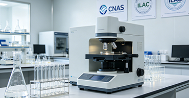
Internationally recognized authority
Certified by multiple international standards such as CNAS, VCS, and GS, with reports universally applicable worldwide.

Global service capability
Covering 140+ countries and regions, it supports on-site detection and remote verification in multiple languages.
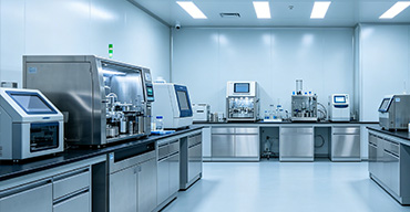
Professional experimental methods
Adopt standard experimental methods to ensure accurate and reliable data.
Advanced Characterization and Performance Evaluation of Titanium Dioxide Thin Films: A Comprehensive Analytical Service
In the realm of functional oxide materials, titanium dioxide (TiO₂) thin films stand as one of the most extensively studied and industrially relevant systems, owing to their exceptional photocatalytic activity, chemical stability, high refractive index, and biocompatibility. However, the macroscopic functional performance of these films is intrinsically governed by a delicate interplay of microstructural parameters—including crystallographic phase composition, grain size, lattice strain, defect chemistry, film thickness, surface roughness, and interfacial quality. Consequently, a rigorous, multi-technique analytical protocol is not merely a quality assurance step; it is a fundamental prerequisite for correlating deposition parameters with targeted applications, ranging from self-cleaning surfaces and photoelectrochemical cells to gas sensors and biomedical coatings.
At our state-of-the-art analytical facility, we offer a fully integrated, ISO/IEC 17025-aligned testing service specifically tailored for titanium dioxide thin films, covering the entire spectrum from nanoscale structural probing to macroscopic optoelectronic and photocatalytic validation. Our service is designed for researchers, process engineers, and product developers who require quantitative, traceable, and interpretable data to accelerate R&D cycles, troubleshoot manufacturing inconsistencies, or certify product compliance.
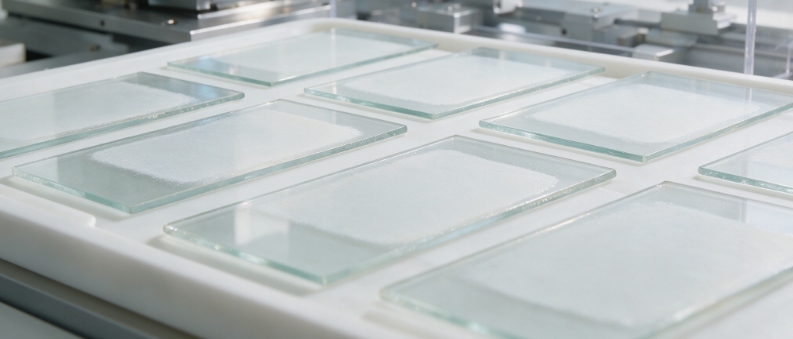
1. Scope of Analytical Capabilities: From Crystallography to Surface Chemistry
Our analytical portfolio for TiO₂ thin films encompasses eight complementary characterization modules, each performed by dedicated specialists using instrumentation maintained under strict environmental controls (temperature, humidity, and vibration isolation). The following core parameters are routinely assessed with certified reference material (CRM) traceability:
Phase identification and quantification: Using high-resolution grazing-incidence X-ray diffraction (GIXRD) with a Cu Kα source and a 2D hybrid pixel detector, we resolve anatase, rutile, and brookite phases with a detection limit below 1 wt%. Rietveld refinement provides unit-cell parameters and anisotropic strain analysis, achieving a lattice parameter accuracy of ±0.0005 Å.
Thickness and density profiling: Via spectroscopic ellipsometry (SE) over the 190–1700 nm range, combined with X-ray reflectometry (XRR), we deliver film thickness (1–1000 nm) with a precision of ±0.1 nm and mass density with an uncertainty of ±0.02 g/cm³. For multilayer or graded-index structures, we apply parametric optical models (Tauc-Lorentz, Cody-Lorentz) to extract both thickness and optical constants (n, k) across the UV-Vis-NIR spectrum.
Surface morphology and roughness: Atomic force microscopy (AFM) in tapping mode, with sub-nanometer vertical resolution, provides root-mean-square roughness (Rq), skewness, and kurtosis over scan areas from 500 nm to 100 µm. For large-area uniformity mapping, we employ white-light interferometry (WLI) to generate 3D topography with a lateral resolution of 0.5 µm.
Chemical bonding and defect states: High-resolution X-ray photoelectron spectroscopy (XPS) with monochromated Al Kα radiation (spot size ≤ 100 µm) identifies Ti 2p, O 1s, and adventitious carbon, with deconvolution of Ti⁴⁺, Ti³⁺, and oxygen vacancy fractions. Depth-profiling via Ar⁺ cluster ion sputtering allows for chemical state mapping through the film–substrate interface, with a sputter rate calibrated against a SiO₂/Si standard.
Optical bandgap and Urbach tail analysis: Using UV-Vis-NIR spectrophotometry with an integrating sphere, we measure total and diffuse transmittance/reflectance. From the Tauc plot (direct and indirect allowed transitions), we determine the optical bandgap (Eg) with a reproducibility of ±0.02 eV, while the Urbach energy (Eᵤ) quantifies sub-bandgap defect disorder down to 10 meV resolution.
Photocatalytic activity under controlled irradiation: We operate a custom-built photoreactor with LED arrays (365 nm, 395 nm, and 450 nm) and an automated gas/liquid sampling system. Using methylene blue or 4-chlorophenol as probe molecules, we extract apparent rate constants (kₐₚₚ) under identical illumination intensity (calibrated with a Si photodiode). This allows direct comparison of intrinsic photoactivity across different film batches, independent of thickness variations.
Electrical and photoelectrochemical properties: For conductive substrates, we perform Hall effect measurements (van der Pauw geometry) to obtain carrier concentration, mobility, and resistivity. In a three-electrode cell, we acquire Mott-Schottky plots to determine flat-band potential and donor density (ND), as well as electrochemical impedance spectroscopy (EIS) over a frequency range of 100 kHz – 10 mHz to separate grain-boundary and bulk charge-transfer resistances.
Adhesion and mechanical integrity: Nanoindentation with a Berkovich tip (load range 0.1–10 mN) yields hardness (H) and reduced elastic modulus (Er), while scratch testing with progressive loading (up to 50 N) quantifies critical loads for cohesive and adhesive failures, following ASTM C1624 standards.
2. Achieving Unprecedented Depth: Advanced Correlative and In-Situ Protocols
Beyond conventional standalone measurements, our laboratory excels in correlative microscopy and spectroscopy that bridges structural, chemical, and electronic information from the same region of interest. For instance, we routinely combine transmission electron microscopy (TEM) with energy-dispersive X-ray spectroscopy (EDS) and electron energy-loss spectroscopy (EELS) on FIB-lifted cross-sections, achieving spatial resolution below 0.2 nm for lattice-fringe imaging and 0.5 nm for chemical mapping. This enables direct observation of interfacial Ti–O coordination changes, grain-boundary segregation, and amorphous interlayers—factors often invisible to bulk diffraction but critical for device performance.
For time-resolved studies, we offer in-situ photocatalytic monitoring under controlled humidity and temperature, coupled with real-time mass spectrometry (MS) to detect volatile organic compound (VOC) degradation intermediates. Furthermore, our variable-angle spectroscopic ellipsometry can be performed in a controlled atmosphere (O₂, N₂, or vacuum) to evaluate photoinduced hydrophilicity and surface reconstruction under UV exposure, providing kinetic data that are indispensable for understanding long-term stability.
To address the growing demand for high-throughput screening, we have developed a automated mapping stage that enables GIXRD, XRR, and SE measurements on up to 100 discrete sample spots per batch, with automated data processing pipelines that generate 2D property maps (e.g., thickness uniformity, phase fraction gradient, and bandgap variation) within 24 hours—a capability that is particularly valuable for sputtering or sol–gel process optimization.
3. Unmatched Data Integrity, Interpretation, and Reporting
What distinguishes our service is not solely the breadth of instrumentation, but the rigorous data science framework applied to every measurement. All raw data are processed using proprietary algorithms that incorporate Monte Carlo uncertainty propagation and multivariate curve resolution (MCR) to deconvolute overlapping spectral features—especially in XPS and Raman spectroscopy. Our final reports include:
Quantitative uncertainty budgets for each derived parameter (e.g., ±0.01 for crystallite size from Scherrer analysis, ±0.05 eV for bandgap), allowing unambiguous comparison with theoretical models or literature values.
Cross-validation using at least two independent techniques for critical parameters (e.g., thickness from SE, XRR, and cross-sectional SEM), with discrepancy analysis to flag potential artefacts such as surface contamination or substrate interference.
Contextual interpretation linking measured properties to deposition conditions (e.g., oxygen partial pressure, substrate temperature, annealing ramp rate) based on our in-house reference database compiled from over 2,000 TiO₂ films produced by ALD, sputtering, CVD, and sol–gel methods. This enables us to provide actionable recommendations for process tuning, rather than mere numerical outputs.
All measurements are performed under accredited quality management (ISO 9001:2015 and IEC 17025 for specific test methods), with regular inter-laboratory comparisons to ensure long-term reproducibility. We also offer customized test plans—for example, accelerated aging tests (humidity-freeze cycles, UV-dosing) followed by re-characterization, to assess reliability in outdoor or biomedical environments.
4. Why Partner with Us for Your TiO₂ Thin Film Analysis
Our competitive edge rests on three pillars: technical depth, operational flexibility, and scientific partnership.
Technical depth: We are one of the few laboratories globally that operate combined XPS–UPS–LEIS (low-energy ion scattering) for true surface-sensitive elemental quantification, and time-of-flight secondary ion mass spectrometry (ToF-SIMS) for 3D molecular imaging with < 1 nm depth resolution. This allows detection of trace contaminants (e.g., alkali ions, residual organics) that can deactivate photocatalytic sites—a diagnostic service rarely offered commercially.
Operational flexibility: We accept samples of any size (from 5 mm × 5 mm fragments to 300 mm wafers) and any substrate (glass, silicon, polymers, metals, flexible foils). For air-sensitive or moisture-sensitive films, we provide inert-atmosphere transfer modules (glovebox-coupled) to avoid surface alteration before analysis. Our typical turnaround time for a full suite is 5–7 business days, with expedited 48‑hour service available for urgent projects.
Scientific partnership: We do not treat analysis as a black-box transaction. Every project is assigned a senior material scientist who consults with you on the most relevant measurement matrix, discusses preliminary results, and refines the plan iteratively. We also offer post‑measurement modelling—including DFT-assisted XPS peak assignment, effective medium approximation (EMA) for porous films, and finite-difference time-domain (FDTD) simulations for light-trapping optimization—to transform raw data into publishable or patentable insights.
Moreover, our pricing model is transparent and modular: you pay only for the modules you need, with volume discounts for long-term collaboration. All data are delivered via a secure cloud portal with raw files (ASCII, .mpt, .vms), processed graphs, and a comprehensive PDF report written in clear, interpretable language—ready for inclusion in regulatory submissions or academic manuscripts.
5. Summary: From Routine Quality Control to Frontier Research
Whether you are a manufacturer seeking batch-to-batch consistency for anti-reflective coatings, a researcher investigating defect-engineered photoelectrodes, or a developer of flexible TiO₂-based sensors, our TiO₂ thin film testing service delivers metrological excellence, interpretative clarity, and actionable intelligence. We have successfully supported over 150 industrial and academic clients across 20 countries, with documented improvements in process yield (by up to 35%) and device efficiency (by up to 18%) through our diagnostic feedback.
We invite you to contact our technical team with your specific film specifications and performance targets. We will provide a detailed proposal outlining the recommended test matrix, expected uncertainties, and a timeline tailored to your decision-making needs. With our combined expertise in surface science, thin-film optics, and catalytic kinetics, we are fully equipped to help you unlock the full potential of your titanium dioxide films—from the atomic scale to the final device application.
Ready to advance your TiO₂ thin film development? Let our analytics drive your next breakthrough.