Reasons for choosing our testing services
ZHONGXI Testing has obtained inspection qualification certifications from multiple countries and regions worldwide. We possess a senior testing team and advanced testing methods, providing independent, impartial, and professional third-party verification services for global carbon projects.
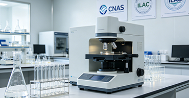
Internationally recognized authority
Certified by multiple international standards such as CNAS, VCS, and GS, with reports universally applicable worldwide.

Global service capability
Covering 140+ countries and regions, it supports on-site detection and remote verification in multiple languages.
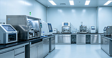
Professional experimental methods
Adopt standard experimental methods to ensure accurate and reliable data.
Advanced Semiconductor Thin-Film Characterization – Comprehensive Metrology and Defect Analysis Services
The performance, yield, and reliability of modern semiconductor devices are increasingly dictated by the quality and consistency of thin films – from gate dielectrics and barrier layers to epitaxial channel stacks and metal interconnects. As device dimensions shrink to single-digit nanometer nodes and new materials (high-κ dielectrics, 2D semiconductors, ferroelectric hafnia, and transition metal dichalcogenides) enter production, the multiparametric characterization of thin films has become a critical enabler for process development, manufacturing control, and failure analysis. Clients seeking thin-film testing services typically aim to: (i) verify thickness, density, and stoichiometry against design targets, (ii) detect and quantify defects (pinholes, voids, roughness, contamination) that impact device leakage or breakdown, (iii) measure electrical properties (resistivity, mobility, dielectric constant, Leakage Current) for device modeling and SPICE extraction, (iv) assess interfacial quality and diffusion barriers for thermal stability, and (v) generate comprehensive material certificates for technology transfers, customer audits, or qualification reports. Our laboratory offers a fully integrated, ISO/IEC 17025-accredited thin-film characterization service that combines non‑destructive metrology, high-resolution microscopy, and quantitative property measurements across a wide range of substrate sizes and film compositions. We deliver not just parameter values, but a unified physical picture that correlates deposition conditions with film properties, enabling our clients to optimize processes with confidence and speed.
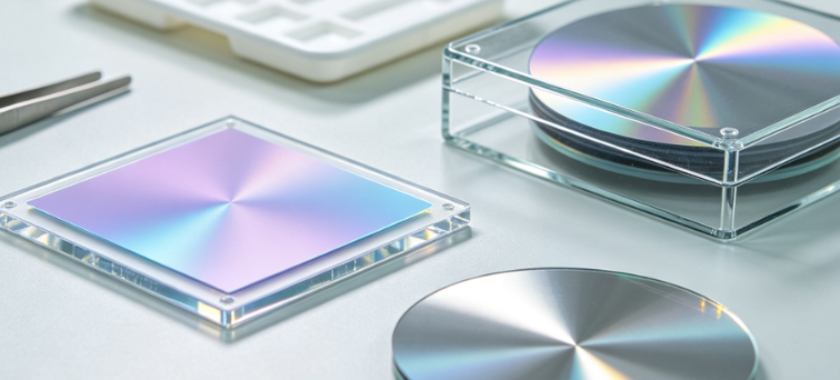
Precision Thickness, Density, and Optical Constant Determination
Accurate film thickness and optical constants (n, k) are fundamental for device design and process control. Our primary platform is a spectroscopic ellipsometry (SE) system (J.A. Woollam RC2-XI) with a wavelength range of 190–1700 nm, equipped with a focusing probe for micro-spot measurements (down to 50 μm) and an autostage for automated mapping. We perform multi-angle SE (45°–75°) with depolarization analysis to simultaneously extract thickness, surface roughness, and graded layer profiles for films ranging from 0.1 nm (interfacial layers) to 20 μm (thick oxides or polymers). For complex stacks (e.g., high-κ / metal gate, ferroelectric HfO₂ with interlayers), we employ advanced optical dispersion models (Tauc-Lorentz, Cody-Lorentz, oscillator combinations) to decouple contributions from multiple layers, providing thickness uncertainty below 0.3% for single layers and <1% for multilayer stacks.
Complementing SE, we use X-ray reflectivity (XRR) on a high-resolution diffractometer (PANalytical X'Pert MRD) to determine film thickness, density, and interface roughness with sub‑nanometer precision. XRR is particularly powerful for films <50 nm thick, where it can resolve the electron density profile and detect subtle density gradients due to porosity or compositional drift. We combine SE and XRR data through simultaneous fitting (genetic algorithm plus Levenberg‑Marquardt) to obtain a self‑consistent thickness and density across the film, minimizing model ambiguity. Our reports include 2D contour maps of thickness and density across the wafer (up to 300 mm), enabling identification of radial non-uniformities from deposition tools.
Crystallinity, Phase Identification, and Stress Analysis
The crystalline structure and stress state of thin films critically affect electrical and mechanical reliability. We perform high-resolution X-ray diffraction (HR-XRD) with a four‑crystal monochromator and a multiple‑axis goniometer, providing θ‑2θ scans, rocking curves (ω‑scans), and reciprocal space maps (RSM) for asymmetric reflections. These measurements yield: (i) phase composition and preferred orientation (texture) via peak identification, (ii) crystallite size and micro‑strain using Williamson‑Hall analysis, (iii) in‑plane and out‑of‑plane lattice parameters, and (iv) biaxial stress (via sin²ψ method or curvature comparison with known bulk values). For polycrystalline or amorphous films, we use grazing‑incidence XRD (GIXRD) with varying incident angles to probe depth‑dependent crystallinity, separating surface and bulk phases. Our stress mapping capability (5 mm spatial resolution) is particularly valuable for films on flexible substrates or for MEMS/NEMS applications, where stress gradient induces bow and warpage.
For films with crystallinity too low for XRD (e.g., ultra‑thin amorphous dielectrics), we employ transmission electron microscopy (TEM) with selected area electron diffraction (SAED) and nanobeam electron diffraction (NBED) on cross‑sectional lamellae, achieving phase identification from 10 nm regions. We also provide Raman spectroscopy with a confocal microscope (532 nm and 785 nm lasers) to detect crystallinity, stress, and doping-induced shifts in semiconductor films (Si, Ge, SiGe, GaN) with a spatial resolution of 0.5 μm.
Chemical Composition, Stoichiometry, and Trace Impurity Analysis
Film stoichiometry and impurity levels are essential for bandgap engineering, doping control, and dielectric reliability. Our chemical analysis suite includes X-ray photoelectron spectroscopy (XPS) with in‑situ ion sputtering for depth profiling (up to 200 nm), providing atomic % of elements and chemical state information (e.g., oxide, nitride, silicate, metal bonding). We quantify the stoichiometry of complex oxides (e.g., Hf1-xZrxO₂, SrTiO₃) and nitrides (TiN, AlN) with accuracies of ±2 at% for major elements and ±0.1 at% for low‑level dopants. For bulk composition, we use Rutherford backscattering spectrometry (RBS) with a 2 MeV He⁺ ion beam, offering accurate areal density (atoms/cm²) and depth profiles (up to 300 nm) without matrix effects, especially useful for heavy elements in light matrices.
Trace impurities (metals, halogens, C, H) are quantified by secondary ion mass spectrometry (SIMS) using a Cameca IMS 7f with both O₂⁺ and Cs⁺ primary beams, achieving detection limits as low as 1×10¹⁵ atoms/cm³ for transition metals and 1×10¹⁸ atoms/cm³ for C and H. We provide full depth profiles (surface to 1 μm) and quantify diffusion coefficients at interfaces. For non‑destructive bulk screening, we employ total reflection X‑ray fluorescence (TXRF) with a detection sensitivity of <1×10¹⁰ atoms/cm² for surface metals. All chemical data are correlated with electrical measurements to identify the root causes of leakage, breakdown, or mobility degradation.
Surface Morphology, Roughness, and Defect Inspection
Surface topography and defect density directly influence yield and device performance. Our primary tool is atomic force microscopy (AFM) (Bruker Dimension FastScan) operating in tapping and peak‑force modes, scanning up to 100 μm with sub‑angstrom vertical resolution. We provide roughness parameters (Ra, Rq, Rz) over multiple scan sizes, power spectral density (PSD) for process fingerprinting, and automated particle/pinhole detection with size and shape classification. For large‑area inspection, we use a laser scanning confocal microscope (Olympus LEXT) and a scanning electron microscope (SEM) with a field‑emission gun (FEI Verios 460) for high‑resolution imaging of sub‑10 nm defects. Automated defect review (ADR) software generates maps of defect type (particles, scratches, pits, delamination), with cross‑sectional FIB‑SEM for in‑depth analysis of critical defects.
For buried interfaces and subsurface defects, we employ scanning acoustic microscopy (SAM) and thermal wave imaging, which detect voids, delaminations, and thickness variations in opaque films such as metals and silicides. Our combined AFM‑SEM‑FIB workflow enables root‑cause analysis from macroscopic contamination down to crystallographic dislocations.
Electrical Characterization – Resistivity, Mobility, Dielectric Constant, and Leakage
Functional films require precise measurement of their electrical properties. We offer a comprehensive electrical test suite using a probe station (Cascade Summit 11000) with temperature control (−40 °C to +200 °C) and a semiconductor parameter analyzer (Keysight B1500A) for DC and pulsed I‑V, C‑V, and transient measurements.
For conductive films (metals, doped semiconductors, transparent conductive oxides): we measure sheet resistance using a four‑point probe and van der Pauw methods, extract resistivity and thickness‑derived conductivity, and perform Hall measurements (van der Pauw with magnetic field up to 1.5 T) to determine carrier concentration and mobility.
For dielectric films: we fabricate metal‑insulator‑metal (MIM) or MIS capacitors and measure capacitance‑voltage (C‑V) at frequencies from 1 kHz to 1 MHz (and up to 10 MHz using an impedance analyzer) to extract dielectric constant (κ), flat‑band voltage, oxide charge density, and interface trap density (Dit using conductance or Terman methods). We also perform voltage‑ramp and time‑dependent dielectric breakdown (TDDB) tests to assess intrinsic breakdown strength (EBD) and long‑term reliability under constant voltage stress (CVS) or constant current stress (CCS). Our TDDB data are analyzed using E‑model and 1/E models to predict operating lifetime under field‑use conditions, with Weibull statistics providing characteristic lifetime and shape parameters.
For ferroelectric and piezoelectric films, we employ a TF Analyzer (aixACCT) for hysteresis (P‑E) and strain (butterfly) measurements, with pulse‑switching and fatigue testing up to 10⁹ cycles.
Interface and Diffusion Barrier Quality – SIMS and TEM-EELS
Interfacial stability and barrier performance are critical for Cu interconnects, metal‑silicide contacts, and high‑κ gate stacks. We use high‑resolution TEM with electron energy loss spectroscopy (EELS) on cross‑sectional lamellae to quantify interfacial layer thickness (e.g., SiO2 at Si/HfO₂, TiN/high‑κ), interdiffusion of elements (e.g., Ti, Al, O), and chemical bonding at the atomic scale. Coupled with energy‑dispersive X‑ray spectroscopy (EDS) mapping in TEM, we provide 2D elemental distribution with 1 nm spatial resolution, detecting early intermetallic formation or segregation of impurities.
For thicker films (>100 nm), we perform Auger depth profiling with continuous sputtering to map interfacial composition and detect barrier failures such as pinholes or Cu penetration. All diffusion data are used to calculate effective diffusion coefficients and activation energies, supporting predictive modeling for process windows.
Thermal Stability and stress relaxation Studies
Thin films undergo significant stress evolution during processing and operation. We offer in‑situ heating experiments on our XRD and ellipsometry platforms, measuring stress, crystallinity, and thickness changes from room temperature up to 1000 °C (in vacuum or controlled atmosphere). This enables the observation of grain growth, phase transitions, stress relaxation, and crystallization kinetics, providing critical input for rapid thermal annealing (RTA) and spike annealing process tuning. Our Wafer curvature measurement system (KLA Tencor FLX) measures substrate curvature at multiple temperatures, extracting stress‑temperature hysteresis loops and revealing viscoelastic behavior.
Our Distinctive Competencies and Added Value
Our semiconductor thin‑film testing service is distinguished by several unique advantages. First, our integrated toolset – spanning ellipsometry, XRR, HR-XRD, XPS, SIMS, TEM, AFM, SEM/FIB, and full electrical characterization – allows us to execute complete cross‑correlative analyses on the same sample site, reducing ambiguity and enabling direct links between structure, chemistry, and function. For example, we can precisely identify the cause of a leakage rise: whether it is due to thickness thinning, elemental diffusion, interfacial roughening, or crystal phase change.
Second, our scientific team includes PhD‑level physicists and materials engineers with extensive experience in advanced nodes (7 nm, 5 nm, 3 nm) and emerging memory technologies (FeRAM, MRAM, ReRAM). We provide expert interpretative consulting that goes beyond data reporting – offering root‑cause hypotheses, process recommendations (e.g., temperature, pressure, precursor flow adjustments), and design of experiments (DoE) for process optimization.
Third, we maintain ISO/IEC 17025 accreditation for thickness, roughness, composition, and electrical measurements, with fully documented uncertainty budgets and NIST‑traceable calibrations. Our laboratory participates in international round‑robins (VLSI Standards, NIST) to ensure our data are comparable with leading fabs and research centers worldwide.
Fourth, we offer rapid turnaround (2–5 business days for standard packages, 1 day for urgent, albeit with prior arrangement) and flexible sample handling: we accept full wafers (2‑12 inch), diced coupons, pieces, and even small (1 mm²) cross‑sections. Our proprietary sample‑mounting and alignment procedures ensure repeatability without damaging the film.
Finally, we provide data security and confidentiality for proprietary material compositions and process conditions, with dedicated project servers, encryption, and signed NDAs.
Comprehensive Service Modules – Tailored to Your Process Stage
We organize our thin‑film testing into modular packages, allowing clients to select the appropriate level of detail:
Module 1 – Physical Dimension and Optical Constants: Spectroscopic ellipsometry (thickness, n,k), XRR (density, roughness), and AFM (RMS roughness, topography) – ideal for initial film qualification and process monitoring.
Module 2 – Crystallographic and Stress Analysis: HR‑XRD (phase, texture, stress), GIXRD (depth‑dependent crystallinity), Raman (stress, crystalline fraction) – essential for anneal optimization and phase control.
Module 3 – Chemical and Compositional Profiling: XPS (stoichiometry, bonding), SIMS (impurity and dopant depth profiles), RBS (elemental areal density), and TXRF (surface metal contamination) – for purity and doping verification.
Module 4 – Electrical and Dielectric Characterization: Resistivity/mobility (4‑point probe, Hall), C‑V (κ, charge, Dit), I‑V (leakage, breakdown), TDDB (lifetime), and ferroelectric hysteresis – for device modeling and reliability assessment.
Module 5 – Defect and Interface Analysis: SEM/ FIB‑SEM (defect review), TEM‑EDS/EELS (interface sharpness, interdiffusion), SAM (delamination/void detection), AFM‑based surface defect mapping – for yield improvement.
Module 6 – Comprehensive Film Qualification Package: All modules combined, plus full data correlation, statistical analysis, and a detailed interpretive report with process recommendations – suitable for new film development, technology transfer, or customer qualification.
Each module includes full documentation, traceability certificates, and a technical summary. We also offer customized test plans for novel materials (e.g., 2D TMDs, oxide‑based ferroelectrics, organic semiconductors) or non‑standard substrates (glass, flexible polymer, SiC, GaN).
Data Integrity and Regulatory Compliance
Our measurements are performed under controlled environment (class 100 cleanroom for sensitive films) and with rigorous standard operating procedures (SOPs). All instruments are calibrated with certified reference materials (NIST, VLSI Standards). Our LIMS records each step, including operator, timestamp, and environmental data. We provide GLP‑compliant reports for regulated applications (automotive, medical, aerospace) with audit‑ready raw data packages. Data is stored securely and is accessible to clients via a protected portal with version control.
Client Engagement and Project Workflow
Our engagement starts with a technical consultation to define your film system, critical parameters, intended application, and any known challenges (e.g., thin layers <3 nm, rough or transparent substrates, air‑sensitive materials). We then propose a tailored test plan with a fixed price and timeline. Upon sample receipt, we perform an incoming visual check and log samples in our LIMS. Testing is executed in parallel where possible, and clients receive progress updates and preliminary data on request. The final deliverable is a comprehensive report with integrated analysis, graphical summaries, uncertainty statements, and expert commentary. We also offer a post‑report review meeting to discuss implications and suggest further experiments.
Conclusion – Empowering Your Thin‑Film Innovation with Unmatched Analytical Depth
As semiconductor devices evolve toward atomic‑scale dimensions and heterogeneous integration, the ability to measure and understand thin films with high precision, cross‑correlated, and time‑efficiently becomes a decisive competitive advantage. Our comprehensive thin‑film characterization service delivers exactly that – a one‑stop, ISO‑accredited solution that transforms multi‑tool data into integrated, physically meaningful insights. With our advanced instrumentation, deep materials expertise, and commitment to client success, we enable fabs, IDMs, and research labs to accelerate development cycles, improve yields, and confidently qualify new processes and materials. Whether you are developing next‑generation gate stacks, advanced barrier layers, or novel memory films, our service provides the clarity and confidence needed to move from deposition to production with assurance.
We invite you to contact our thin‑film characterization specialists to discuss your specific needs. Let us partner with you to unlock the full potential of your films – from the first calibration run to full‑scale manufacturing. Your journey to superior thin‑film performance begins with our rigorous, insightful, and actionable testing.