Reasons for choosing our testing services
ZHONGXI Testing has obtained inspection qualification certifications from multiple countries and regions worldwide. We possess a senior testing team and advanced testing methods, providing independent, impartial, and professional third-party verification services for global carbon projects.

Internationally recognized authority
Certified by multiple international standards such as CNAS, VCS, and GS, with reports universally applicable worldwide.

Global service capability
Covering 140+ countries and regions, it supports on-site detection and remote verification in multiple languages.

Professional experimental methods
Adopt standard experimental methods to ensure accurate and reliable data.
Comprehensive Characterization and Reliability Testing for Semiconductor Light-Emitting Devices – Advanced Optoelectronic Assessment Services
Semiconductor light-emitting devices – including light-emitting diodes (LEDs), laser diodes (LDs), superluminescent diodes (SLDs), and vertical‑cavity surface‑emitting lasers (VCSELs) – are the foundational building blocks of modern illumination, display, communication, and sensing systems. As these devices migrate to higher power densities, tighter wavelength tolerances, and more demanding application environments (automotive, aerospace, biomedical, and quantum technology), the multiparametric, failure‑aware characterization of their electrical, optical, thermal, and reliability attributes has become an indispensable requirement for product development, manufacturing control, and customer acceptance. Clients seeking such testing services typically aim to: (i) validate device performance against design targets and industry standards (e.g., IES, CIE, JEDEC, AEC‑Q102), (ii) screen for early‑life failures and degradation mechanisms via accelerated stress tests, (iii) quantify spectral stability, color consistency, and efficiency droop under realistic operating conditions, (iv) optimize thermal management by measuring junction temperature and thermal resistance, and (v) generate comprehensive qualification data for technical datasheets, regulatory submissions, and customer audits. Our laboratory offers a fully integrated, ISO/IEC 17025‑accredited optoelectronic testing service that combines precision electro‑optical metrology, time‑resolved and temperature‑dependent measurements, and reliability physics analysis into a unified assessment platform. We do not merely report pass/fail metrics; we deliver a predictive performance fingerprint that correlates structural parameters with functional degradation, enabling our clients to optimize epitaxy, chip design, and packaging with unprecedented clarity and confidence.
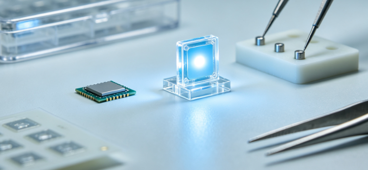
Full Electro‑Optical Parameter Suite – Static, Pulsed, and Spectral Characterization
Our primary characterization platform is an integrated automated probe station (Cascade Summit 12000) coupled with a high‑speed source‑measure unit (Keysight B1500A and Keithley 2657A) and a calibrated spectroradiometer (Instrument Systems CAS 140D) housed within an integrating sphere (1.5 m diameter) for absolute flux and radiance measurements. This configuration enables simultaneous acquisition of over 40 device parameters, including: forward voltage (VF) at multiple current levels (from 1 µA to 10 A), series resistance, ideality factor, threshold current (for lasers), radiant flux (mW), luminous flux (lm), peak wavelength (λp), dominant wavelength (λd), spectral power distribution (SPD) from 200 nm to 1700 nm, full width at half maximum (FWHM), color coordinates (CIE 1931 and 1976), correlated color temperature (CCT), color rendering index (CRI – Ra and R1‑R15), chromaticity difference (Duv), and polarization degree (for LDs). All measurements are performed at four controlled junction temperatures (25 °C, 55 °C, 85 °C, and 105 °C) using a thermoelectric chuck (TEC) with ±0.2 °C stability, enabling the extraction of temperature coefficients for VF (mV/°C) and wavelength (nm/°C) – essential data for system‑level thermal compensation and lifetime estimation.
For high‑speed applications such as visible light communication (VLC), Li‑Fi, and pulse‑driven sensing, we offer dynamic electro‑optical characterization using a 1.5 GHz bandwidth oscilloscope (LeCroy WavePro) and a programmable pulse generator (with rise time < 200 ps). This captures rise/fall times (tr, tf), modulation bandwidth (‑3 dB cut‑off frequency), relative intensity noise (RIN), and latency jitter under various duty cycles and modulation formats (NRZ, PAM‑4). For VCSELs and edge‑emitting lasers, we measure light‑current‑voltage (L‑I‑V) curves in both continuous‑wave (CW) and pulsed modes (with pulse widths down to 50 ns) to separate self‑heating effects from intrinsic efficiency. Our system also performs spatial far‑field and near‑field pattern mapping using a goniometric setup with a motorized rotating stage, providing angular intensity distribution, beam divergence, and M² beam quality factor – critical for optical system design.
Thermal Resistance and Junction Temperature Analysis
Junction temperature (Tj) is the single most influential parameter for device efficiency, wavelength stability, and lifetime. Our laboratory employs two complementary thermal measurement techniques to ensure accuracy across all device types and packaging configurations. The first is the forward‑voltage temperature coefficient (K‑factor) method, which uses the diode itself as a temperature sensor: we calibrate VF against Tj (from 20 °C to 120 °C) using a temperature‑controlled oven, then apply a low‑sensing current to measure Tj during operation with ±0.3 °C accuracy. The second is thermal impedance spectroscopy using a T3Ster® transient thermal tester, which records the electrical cooling curve after a step current and performs structure‑function analysis to resolve the thermal resistance network: junction‑to‑case (RθJC), case‑to‑solder (RθCS), solder‑to‑board (RθSB), and total junction‑to‑ambient (RθJA). We provide cumulative structure functions and differential thermal capacitance plots, which pinpoint the exact bottleneck in the heat dissipation path – whether it is die attach voiding, solder delamination, or insufficient heatsinking. This diagnostic capability is invaluable for packaging optimization and for comparing different thermal interface materials (TIMs).
All thermal measurements are performed under still‑air, forced‑air (0.5–5 m/s), and liquid‑cooled conditions, using a wind tunnel that we have designed to mimic various application environments (automotive engine compartments, outdoor luminaires, data‑center optical modules). We also measure thermal droop – the reduction in optical output with increasing current – by comparing CW and pulsed (0.1% duty cycle) L‑I curves at identical Tj, separating the efficiency loss due to high current density from that due to self‑heating. This allows clients to independently optimize their epitaxial structure (to reduce Auger and defect‑related droop) and their packaging (to lower RθJA).
Reliability and Lifetime Testing – Accelerated Stress and Physics‑of‑Failure Modeling
Reliability qualification is the cornerstone of market acceptance for semiconductor light‑emitting devices, particularly for automotive, aerospace, and outdoor lighting applications where failures are costly and safety‑critical. Our reliability testing suite is fully compliant with IES LM‑80 (lumen maintenance), TM‑21 (extrapolation), AEC‑Q102 (automotive optoelectronics), and JEDEC JESD22 standards, and we go beyond them by incorporating multi‑stress combinatorial protocols. We operate a dedicated reliability chamber farm with 96 individually addressable test slots, each capable of independent current (up to 10 A), temperature (up to 150 °C), and humidity (10–95% RH) control, allowing simultaneous execution of:
(i) Constant current aging at three junction temperatures (55 °C, 85 °C, and 105 °C) for a minimum of 6,000 hours (per LM‑80), with in‑situ monitoring of VF and relative optical power (via calibrated photodiodes). We log data at 1‑minute intervals, capturing transient spikes or gradual degradation.
(ii) Thermal cycling (−40 °C to +125 °C, 1,000 cycles, dwell time 15 min, ramp rate 15 °C/min) to evaluate solder joint fatigue, wire‑bond integrity, and encapsulant cracking.
(iii) Humidity‑temperature‑bias (HTB) at 85 °C/85% RH with reverse bias (AEC‑Q102 condition) to assess electrochemical migration and corrosion of metallization.
(iv) Power cycling with 1‑minute on/off sequences to simulate real‑world switching loads, which often reveal thermal‑mechanical failure modes not observed in constant‑current tests.
All aging data are processed by our proprietary degradation modeling platform, which fits both the Arrhenius temperature acceleration and the Eyring‑based combined‑stress model, extracting activation energy (Ea) for each degradation mechanism (e.g., defect propagation, phosphor degradation, Ohmic contact degradation). We then use these kinetic parameters to predict L70 (time to 70% lumen maintenance), L50, and even the time to catastrophic failure (e.g., sudden VF drop) under user‑specified operating profiles (e.g., 50 °C ambient, 70% duty cycle). Our model outputs include confidence intervals and sensitivity analyses, enabling clients to make risk‑based decisions on warranty periods and field‑return strategies.
Advanced Spectral and Color Stability Under Stress
Beyond lumen maintenance, many applications demand strict color stability – especially in display backlighting, museum lighting, and medical imaging. During all reliability tests, we perform periodic high‑resolution spectroradiometry (at 500‑hour intervals) to track peak wavelength shift, FWHM broadening, color coordinate drift (Δu’v’), CCT change, and CRI degradation. We separate the contributions of the active region (blue pump) and the phosphor converter (for white LEDs) via spectral deconvolution, allowing us to pinpoint whether degradation is due to quantum well intermixing, carrier leakage, or phosphor thermal quenching. For RGB and multi‑chip modules, we measure the individual color channel stability and the resulting white‑point shift under mixed‑drive conditions. Our proprietary algorithm correlates these spectral shifts with the thermal impedance data to establish a predictive model for color maintenance, providing clients with actionable guidelines for derating or active temperature compensation.
ESD Susceptibility and Electrical Overstress (EOS) Tolerance
Electrostatic discharge (ESD) and electrical overstress are among the most common causes of premature field failures in semiconductor optoelectronics. Our ESD testing capability covers both human body model (HBM) and charged device model (CDM) per ANSI/ESDA/JEDEC JS‑001 and JS‑002, with pulse voltages up to ±8 kV (HBM) and ±2 kV (CDM). We perform I‑V curve tracing and electroluminescence (EL) imaging before and after each stress pulse to detect subtle damage (e.g., micro‑cracks, current crowding, or leakage path formation) that may not manifest as immediate catastrophic failure but reduces device lifetime. For EOS, we apply current or voltage ramps (up to 2× rated values) with variable rise times, monitoring the L‑I‑V characteristics in real time to determine the safe operating area (SOA) and the failure threshold energy. These data are critical for designing protection circuits and for setting absolute maximum ratings in datasheets.
Failure Analysis and Root‑Cause Diagnostics
When devices fail or exhibit performance drift beyond acceptable limits, our integrated failure analysis (FA) service combines non‑destructive and destructive techniques to identify the precise origin. Our FA workflow includes:
(i) Optical and confocal microscopy for visual inspection of the chip surface, bonding wires, and phosphor layer – detecting burn marks, cracks, or discoloration.
(ii) Scanning electron microscopy (SEM) with energy‑dispersive X‑ray spectroscopy (EDS) for high‑magnification imaging and elemental analysis of degraded regions (e.g., Au‑Al intermetallic voids, Ag migration, or die‑attach delamination).
(iii) Focused ion beam (FIB) cross‑sectioning combined with TEM and SAED to examine the quantum well structure, dislocation networks, and interfacial reactions at the nanoscale – revealing whether degradation originated from epitaxial defects, contact degradation, or phosphor damage.
(iv) Infrared (IR) thermography and micro‑photoluminescence (µ‑PL) mapping to localize hot spots and non‑radiative recombination zones, correlating thermal and optical non‑uniformities.
We integrate all FA data with the device’s pre‑failure electro‑optical and thermal history to construct a complete failure timeline, attributing the root cause to specific materials, process steps, or application conditions. This level of diagnostic depth is rarely available in commercial test houses and is highly valued by clients involved in product liability disputes, warranty returns, or continuous improvement programs.
Compliance with International Standards and Traceability
All our measurements are conducted in accordance with IES LM‑79, LM‑80, CIE S 025, JEDEC JESD51, AEC‑Q102, and ISO 14717 standards, where applicable. Our laboratory is accredited to ISO/IEC 17025 for optoelectronic parameter measurement, and we maintain NIST‑traceable calibration for all radiometric, photometric, and electrical references. We participate in annual interlaboratory comparison programs (e.g., NIST LED characterization, PTB cross‑calibration) to ensure global comparability. Our reports include detailed uncertainty budgets (expanded uncertainty, k=2) for each reported parameter – typically below 2% for flux and 0.2 nm for wavelength – providing transparency and confidence for regulatory submissions and customer audits.
Our Distinctive Competencies – Integration, Physics‑Based Insight, and Partnership
Our service is distinguished by several unique advantages that reflect our deep expertise in semiconductor photonics. Firstly, our team comprises PhD‑level device physicists and reliability engineers with direct experience in epitaxial growth, chip processing, and packaging – enabling us to interpret measurement data not just as numbers, but as signatures of underlying physical mechanisms. We can, for instance, distinguish between a degradation caused by defect propagation from that caused by contact degradation, and recommend specific corrective actions (e.g., adjusting the V/III ratio, modifying the contact alloy temperature, or changing the bonding parameter).
Secondly, we offer a truly integrated multi‑modal platform where electrical, optical, thermal, and reliability tests are performed on the same set of devices within the same facility. This eliminates inter‑tool variability and provides direct correlations – for example, between thermal resistance and wavelength drift, or between ESD sensitivity and forward‑voltage ideality. Our data analysis pipeline applies machine learning clustering to automatically group devices by performance signatures, revealing hidden patterns that are not discernible from single‑parameter testing.
Thirdly, we invest in custom test fixtures and cryogenic/ambient probes for unconventional devices, such as micro‑LEDs (down to 5 μm pitch), VCSEL arrays, and ultraviolet (UV) LEDs (with quartz windows). Our in‑house mechanical workshop can design and fabricate specialized sockets and temperature‑controlled mounts within a week, ensuring rapid turnaround for prototype evaluation.
Fourthly, we offer remote monitoring and control – clients can log into our testing platform via a secure VPN to view real‑time data, adjust test parameters, or perform on‑the‑fly analysis. This transparency builds trust and accelerates decision‑making, particularly during critical development phases.
Finally, our consultative approach includes a comprehensive review session after each project, where we present not only the test results but also our interpretation, compare them with industry benchmarks, and suggest follow‑up experiments or design modifications. We view ourselves as a technical partner, not just a test service, and many of our clients rely on us for long‑term reliability roadmaps and qualification strategy planning.
Comprehensive Service Modules – Customized to Your Device Type and Application
We structure our testing into modular packages, allowing you to select the exact scope needed for your project:
Module 1 – Basic Electrical and Optical Characterization (LM‑79 compliant): VF, luminous/radiant flux, CCT, CRI, color coordinates, and spectral power distribution at 2–3 current levels – ideal for datasheet generation and batch screening.
Module 2 – Thermal Characterization and Droop Analysis: K‑factor calibration, Tj measurement, RθJC/RθJA via structure functions, pulsed vs. CW L‑I‑V comparison – essential for thermal design validation.
Module 3 – Dynamic and High‑Frequency Testing: Rise/fall times, modulation bandwidth, RIN, and eye diagram (for communication devices) – critical for VLC, Li‑Fi, and optical transceiver applications.
Module 4 – Reliability and Lifetime Qualification (LM‑80 + TM‑21): 6,000‑hour aging at 3 temperatures, with periodic measurements, plus Weibull and Arrhenius analysis to predict L70/L50 – the industry standard for warranty and certification.
Module 5 – Environmental and Mechanical Stress Testing: Thermal cycling, HTB, power cycling, ESD (HBM/CDM), and vibration/shock (per AEC‑Q102) – for automotive and industrial grade components.
Module 6 – Comprehensive Qualification Package: All modules combined into a single project, including a final integrated report with statistical analysis, degradation mode differentiation, and actionable recommendations – suitable for new product launch, supplier approval, or regulatory compliance.
Module 7 – Failure Analysis and Root‑Cause Investigation: Full FA workflow (optical, SEM/EDS, FIB‑TEM, IR thermography, µ‑PL) with a detailed forensic report – for return analysis or troubleshooting.
We accept single devices, packaged modules, arrays, and even un‑packaged bare die (with appropriate probing). Minimum sample requirements vary by test – we provide guidance during the consultation. We offer flexible pricing based on volume, repeat testing, and long‑term contracts.
Data Integrity, Security, and Confidentiality
We strictly adhere to ALCOA+ principles for data integrity. All instrument raw files, logs, and operator entries are stored in a secure, version‑controlled electronic data management system with full audit‑trail. Any manual annotation or outlier rejection is documented and authorized. Our IT infrastructure is protected by multi‑layer firewalls, encrypted data transfer, and role‑based access. We sign non‑disclosure agreements (NDAs) with all clients and treat test results, device designs, and proprietary information as strictly confidential. For clients with high‑security requirements (e.g., military or aerospace), we offer off‑line analysis and paper‑based reporting options.
Client Engagement and Workflow
Our engagement process is designed for efficiency and clarity. It begins with a pre‑project consultation – typically a 30‑minute call – where we define your device type, intended application, critical parameters, and applicable standards. We then prepare a tailored test plan, a fixed‑price quotation, and a detailed sample handling guide (e.g., ESD precautions, orientation marking, storage conditions). After receiving your samples, we log them in our LIMS, perform incoming visual inspection, and start testing according to the agreed schedule. Clients receive real‑time progress updates through our secure portal, with optional preliminary data sharing at intermediate milestones. The final report is delivered as a structured PDF, supplemented with editable raw data files (Excel/CSV) and graphical summaries. We also include a post‑delivery debrief meeting to walk through the results, highlight key findings, and discuss potential actions or further studies.
Conclusion – Advancing Your Semiconductor Lighting Technology with Uncompromising Testing Excellence
Semiconductor light‑emitting devices are at the heart of tomorrow's energy‑efficient, intelligent, and high‑speed optical systems. Their successful market deployment, however, relies on a thorough understanding of their electrical, optical, thermal, and reliability behavior under realistic and extreme conditions. Our comprehensive testing service provides exactly that – a one‑stop, ISO‑accredited, physics‑based solution that transforms measurement data into predictive intelligence. With our state‑of‑the‑art instrumentation, deep domain expertise, and client‑centric partnership model, we empower device manufacturers, integrators, and end‑users to accelerate development, reduce field failures, and confidently differentiate their products in a competitive landscape.
We invite you to contact our optoelectronic testing specialists to discuss your specific needs, whether you are qualifying a new VCSEL for automotive LiDAR, optimizing the color stability of a high‑CRI LED, or verifying the reliability of a micro‑LED array for augmented reality. Let us partner with you to illuminate the full potential of your semiconductor light‑emitting devices – from the first prototype to mass production and beyond. Your journey to optoelectronic excellence starts with our rigorous, insightful, and actionable testing.