Reasons for choosing our testing services
ZHONGXI Testing has obtained inspection qualification certifications from multiple countries and regions worldwide. We possess a senior testing team and advanced testing methods, providing independent, impartial, and professional third-party verification services for global carbon projects.

Internationally recognized authority
Certified by multiple international standards such as CNAS, VCS, and GS, with reports universally applicable worldwide.

Global service capability
Covering 140+ countries and regions, it supports on-site detection and remote verification in multiple languages.

Professional experimental methods
Adopt standard experimental methods to ensure accurate and reliable data.
Comprehensive Characterization and Reliability Assessment for Nitride Semiconductor Devices – Advanced Testing Services
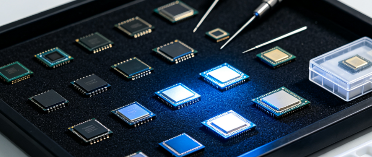
Nitride semiconductors – encompassing gallium nitride (GaN), aluminum nitride (AlN), indium nitride (InN), and their ternary and quaternary alloys – have established themselves as the materials of choice for a broad spectrum of high‑performance electronic and optoelectronic devices, including high‑electron‑mobility transistors (HEMTs), light‑emitting diodes (LEDs), laser diodes, ultraviolet (UV) photodetectors, and power switches. The unique combination of a wide bandgap, high breakdown field, high electron saturation velocity, and strong polarization effects enables devices that outperform conventional silicon and gallium arsenide technologies in terms of power density, frequency, and efficiency. However, the complexity of nitride heterostructures, the presence of high densities of threading dislocations, the sensitivity of the two‑dimensional electron gas (2DEG) to interfacial roughness, and the susceptibility to trapping and reliability degradation demand a multidimensional, multiscale, and physics‑based testing approach. Clients seeking nitride device testing services typically aim to: (i) verify device performance (DC, RF, power, and optical) against design specifications and industry standards (e.g., JEDEC, AEC‑Q101, MIL‑STD), (ii) screen for early‑life failures and degradation mechanisms via accelerated stress tests, (iii) characterize trapping, temperature, and frequency dependence of key parameters (RON, Vth, transconductance, efficiency), (iv) evaluate the robustness of contacts, passivation, and field plates under harsh operating conditions, (v) perform failure analysis to identify root causes of parametric drift or catastrophic breakdown, and (vi) generate comprehensive qualification data for product datasheets, customer audits, and regulatory submissions (e.g., for automotive or aerospace applications). Our laboratory offers a fully integrated, ISO/IEC 17025‑accredited nitride device testing service that combines DC and pulsed I‑V, RF small‑signal and large‑signal, high‑voltage breakdown, capacitance‑voltage (C‑V), deep‑level transient spectroscopy (DLTS), optical output, and thermal impedance measurements with physics‑based modeling and failure analysis. We go beyond standard pass/fail testing to deliver a predictive performance and reliability fingerprint that correlates material properties, process parameters, and device architecture with operational stability and lifetime, enabling clients to optimize design, improve yield, and accelerate time‑to‑market.
DC and Pulsed Current‑Voltage Characterization – Static and Dynamic Performance
Fundamental to any nitride device evaluation is the accurate measurement of DC transfer and output characteristics. Our testing platform comprises a high‑voltage semiconductor parameter analyzer (Keysight B1505A) with high‑power source‑measure units (up to 1500 V and 50 A) and a temperature‑controlled probe station (Cascade Summit 12000) covering –60 °C to +300 °C. We perform ID‑VDS, ID‑VGS, and IG‑VGS measurements on HEMTs, I‑V on diodes, and L‑I‑V on LEDs and laser diodes. For HEMTs, we extract key parameters: threshold voltage (Vth), on‑resistance (RON), transconductance (gm), output conductance, subthreshold swing, and gate leakage. To separate self‑heating effects from intrinsic device response, we perform pulsed I‑V measurements with pulse widths from 200 ns to 10 µs and duty cycles as low as 0.01%, using a high‑speed pulse generator and a digitizing oscilloscope synchronized with the SMUs. This allows us to extract the isothermal I‑V characteristics and quantify the thermal resistance (Rth) from the difference between DC and pulsed curves.
For power devices, we perform off‑state Breakdown Voltage (VBD) and Leakage Current measurements up to 1500 V, with temperature dependence to determine the avalanche capability and the impact of trapping on dynamic RON. For optoelectronic devices, we measure the light output power vs. current (L‑I) and external quantum efficiency (EQE) using a calibrated integrating sphere, and we correlate the electrical parameters with optical performance to identify efficiency droop mechanisms.
RF Small‑Signal and Large‑Signal Characterization – S‑Parameters, Power, and Linearity
For high‑frequency applications (5G, radar, satellite communications), we offer a comprehensive RF testing suite up to 110 GHz using a vector network analyzer (VNA) (Keysight PNA‑X) and a pulsed‑RF measurement system. We perform S‑parameter measurements (5 to 110 GHz) under different bias conditions and temperatures, extracting small‑signal parameters: cut‑off frequency (fT), maximum oscillation frequency (fmax), gain (|S21|), and stability factor (K). We also perform load‑pull and source‑pull measurements using an automated tuner system to determine the optimal impedance for maximum output power, power‑added efficiency (PAE), and linearity. For large‑signal characterization, we measure output power (Pout), gain compression, and third‑order intermodulation distortion (IMD3) as a function of input power and bias, providing critical data for power amplifier design. Our system is equipped with harmonics measurement capability, enabling the analysis of nonlinearity and the extraction of large‑signal model parameters (e.g., Angelov, EEHEMT) for circuit simulation.
Capacitance‑Voltage (C‑V) and Deep‑Level Transient Spectroscopy (DLTS) – Trapping and Interface States
Trapping effects are a major reliability concern in nitride devices, causing current collapse, dynamic RON increase, and threshold voltage instability. We perform C‑V measurements (1 kHz to 10 MHz) on Schottky and MOS capacitors to extract the carrier concentration profile, built‑in potential, and interface trap density (Dit) using the Terman and conductance methods. For deeper trap characterization, we employ deep‑level transient spectroscopy (DLTS) with a temperature range of 77 K to 500 K and a filling pulse width from 1 µs to 100 ms. We identify the activation energy (Ea), capture cross‑section, and trap concentration of each defect level, correlating them with known trap signatures (e.g., carbon‑related, nitrogen‑vacancy, Fe‑related). We also perform isothermal transient spectroscopy (ITS) to study trapping dynamics under real‑time bias conditions. Our advanced analysis includes the Laplace DLTS technique for resolving closely spaced trap levels, providing a comprehensive trap inventory that is essential for reliability prediction.
We complement this with frequency‑dependent conductance measurements to separate the contributions of surface states and bulk traps, and we use pulsed C‑V with sub‑microsecond rise times to study fast trapping events that affect switching performance.
Thermal Characterization and Junction Temperature Measurement
The self‑heating effect in nitride devices is severe due to the high power density and the relatively low thermal conductivity of substrates (especially GaN‑on‑Si). We perform thermal resistance (Rth) measurement using the transient thermal impedance method (T3Ster® system), which applies a step current and records the cooling curve of the forward voltage (or drain saturation current) to derive the structure function and the cumulative thermal resistance network (junction‑to‑case, case‑to‑ambient). We also employ infrared (IR) thermography with a spatial resolution of 5 µm and a temporal resolution of 1 ms to map the temperature distribution across the active area under actual bias, identifying hot spots that may lead to local degradation. For HEMTs, we use the gate‑metal resistance temperature coefficient (or the Vth shift at low current) to estimate the channel temperature with high accuracy (±1 °C). Our thermal analysis also includes thermal cycling (−40 °C to +150 °C, up to 2000 cycles) to evaluate the thermal‑mechanical fatigue of contacts and interconnects.
Reliability and Lifetime Testing – Accelerated Stress and Physics‑of‑Failure Modeling
Reliability qualification is a critical step for nitride device adoption in demanding applications. We operate a dedicated multi‑site reliability test system capable of applying constant current, constant voltage, or pulsed stress to up to 96 devices simultaneously, with independent temperature control (up to 300 °C) and humidity (10‑95% RH). We perform the following accelerated stress tests:
(i) High‑temperature reverse bias (HTRB) – to evaluate the stability of the drift region and the passivation.
(ii) High‑temperature gate bias (HTGB) – to assess gate oxide or Schottky contact degradation.
(iii) Power cycling with a typical on‑time of 1‑5 minutes and off‑time of 1‑2 minutes to simulate application conditions.
(iv) Humidity‑temperature‑bias (HTB) (85 °C/85% RH) with bias to evaluate electrochemical corrosion.
(v) ESD (HBM and CDM) per ANSI/ESDA/JEDEC standards to assess robustness.
During stress, we periodically measure DC, RF, and optical parameters (for LEDs) to monitor degradation. We analyze the degradation kinetics using Arrhenius, Eyring, and power‑law models, extracting the activation energy (Ea) and the lifetime (L10, L50) at use conditions. Our proprietary physics‑of‑failure (PoF) framework combines experimental data with TCAD simulations to identify the dominant failure mechanisms (e.g., hot‑electron injection, trap generation, contact spiking, or die‑attach voiding) and to provide guidelines for derating or design improvement.
Optical and Electroluminescence Characterization for Emitting Devices
For GaN‑based LEDs and laser diodes, we perform a full suite of optical measurements, including electroluminescence (EL) spectra (350‑1700 nm) as a function of current and temperature, light output power (L‑I) and EQE measurements using an integrating sphere, and spatial far‑field pattern using a goniometric scanner. We measure peak wavelength, FWHM, CCT, and CRI for white LEDs, and we perform temperature‑dependent EL (‑40 °C to +125 °C) to determine the wavelength‑shift coefficient and the efficiency droop behavior. For laser diodes, we measure L‑I‑V under CW and pulsed conditions, threshold current (Ith), slope efficiency, and polarization. We also perform linewidth measurement using a high‑resolution optical spectrum analyzer. All optical data are correlated with the electrical and thermal data to provide a complete device quality assessment.
Failure Analysis – From Electrical Faults to Physical Root Causes
When devices fail to meet specifications or exhibit unexpected degradation, our failure analysis (FA) service provides a systematic, multi‑technique investigation. Our FA flow includes:
(i) Electrical characterization to confirm the failure mode (e.g., increased leakage, open circuit, degraded RON).
(ii) Optical inspection to detect visible damage (burn marks, cracks, discoloration).
(iii) Scanning electron microscopy (SEM) with EDS for imaging and elemental analysis of the gate, source, drain, and contact pads.
(iv) Focused ion beam (FIB) cross‑sectioning followed by TEM to examine the gate metal, barrier layer, 2DEG interface, and substrate‑epitaxy interface at the atomic scale, revealing dislocation clusters, gate‑metal interdiffusion, or void formation.
(v) Scanning probe techniques (AFM, KPFM) to map surface potential and workfunction changes.
(vi) Electroluminescence (EL) and photoluminescence (PL) imaging to locate non‑radiative regions in LED failures.
We combine these data to reconstruct the failure timeline and determine the root cause – whether it is process‑induced (e.g., gate recess damage), material‑related (e.g., dislocations), or application‑driven (e.g., overstress). Our reports include a clear conclusion and recommended corrective actions, such as changing the passivation dielectric, adjusting the gate field plate design, or modifying the ohmic contact annealing.
Our Distinctive Competencies – Integration, Physics‑Based Insight, and Global Traceability
What sets our nitride device testing service apart is the seamless integration of electrical, thermal, optical, and physical characterization within a single laboratory, combined with a strong foundation in nitride device physics. Our team comprises PhD‑level researchers and engineers with extensive experience in GaN HEMTs, LEDs, and power devices, including design, fabrication, and modeling. We do not simply report numbers; we interpret them in terms of underlying mechanisms – for example, distinguishing between trap‑related current collapse and thermal‑related degradation, or differentiating between interface roughness scattering and alloy disorder scattering in mobility reduction.
Our laboratory is ISO/IEC 17025 accredited for many of the test methods (I‑V, C‑V, S‑parameters, HTRB, HTGB), and we maintain NIST‑traceable calibrations for all equipment. We participate in international round‑robins (e.g., JEDEC JC‑70, IEEE PELS) to ensure our measurement procedures and data are comparable with leading labs worldwide. We offer rapid turnaround (3‑5 business days for standard DC and RF tests, 2‑3 weeks for reliability tests) and flexible sample handling, accepting bare die, packaged devices, or full wafers (up to 200 mm).
We also provide custom test development for emerging nitride devices (e.g., vertical GaN FETs, AlGaN‑based solar‑blind detectors, GaN‑on‑SiC for radar) and for non‑standard operating conditions (e.g., cryogenic temperatures, high‑voltage pulse trains). Our data analytics platform employs machine learning to identify subtle correlations between process parameters and device characteristics, helping clients accelerate process optimization and yield improvement.
Comprehensive Service Modules – Tailored to Your Device Type and Lifecycle
We structure our testing into modular packages to meet diverse client needs:
Module 1 – Basic DC and Pulsed I‑V Characterization: ID‑VDS, ID‑VGS, RON, Vth, gm, Breakdown Voltage, and leakage – essential for parameter extraction and initial device sorting.
Module 2 – RF Small‑Signal (S‑parameters) and Large‑Signal (Load‑Pull): fT, fmax, Pout, PAE, gain compression, IMD3 – for communication and radar device qualification.
Module 3 – Trapping and Interface Characterization: C‑V (Dit, carrier profile), DLTS (trap energy, capture cross‑section), pulsed C‑V, and conductance method – for trapping analysis and reliability prediction.
Module 4 – Thermal Characterization: Rth measurement, IR thermography, temperature‑dependent I‑V, and thermal impedance spectroscopy – for thermal management validation.
Module 5 – Reliability and Lifetime Testing: HTRB, HTGB, HAST, power cycling, ESD, and Weibull/Arrhenius analysis – for qualification and lifetime prediction.
Module 6 – Optical and Electroluminescence Assessment: L‑I‑V, EL spectra, color parameters (CCT, CRI), wavelength vs. temperature, and far‑field pattern – for LED and laser diode performance.
Module 7 – Failure Analysis and Root‑Cause Investigation: SEM/EDS, FIB‑TEM, EL/PL imaging, KPFM, and comprehensive forensic reporting – for return analysis and process improvement.
Module 8 – Comprehensive Device Qualification Package: All modules combined into a single project, with integrated correlation analysis, statistical summary, and a detailed interpretive report – suitable for product release, customer audits, or regulatory submissions.
We also offer custom test plans for special requirements, such as radiation hardness evaluation, TID (total ionizing dose) testing, or high‑temperature gate‑switching tests.
Data Integrity, Security, and Reporting
All measurements are performed under strict SOPs, with fully traceable calibration records and environmental logging. Our Laboratory Information Management System (LIMS) records every operation, operator, and timestamp, ensuring full auditability. We use encrypted data transfer and role‑based access to protect client proprietary information. Our reports include comprehensive tables, 2D/3D graphs, uncertainty budgets, and an executive summary that translates technical findings into actionable business insights. We provide raw data files (CSV, Excel) upon request. A post‑delivery review meeting is included to discuss results and recommend next steps.
Client Engagement and Workflow
Our engagement begins with a complimentary consultation to define your device type, application, critical parameters, and any specific concerns (e.g., short‑channel effects, thermal crowding, or dynamic degradation). We then propose a tailored test plan with a fixed price and timeline. Upon sample receipt (we accept die, packages, or wafers), we log and inspect the samples, then commence testing. Clients receive progressive updates through our secure portal, with preliminary data shared on request. The final report is delivered in PDF format, and we offer a follow‑up call to discuss the findings and their implications for your development or production.
Conclusion – Empowering Your Nitride Device Technology with Unrivaled Testing Excellence
Nitride semiconductor devices represent a paradigm shift in power electronics, RF communications, and solid‑state lighting, but their full potential can only be realized through rigorous, multidimensional, and physics‑based characterization across all stages of development, from epitaxy to packaging. Our comprehensive testing service provides exactly that – a one‑stop, ISO‑accredited solution that delivers not only accurate measurements but also deep insights into device behavior, degradation mechanisms, and reliability margins. With our advanced instrumentation, experienced scientific team, and unwavering commitment to quality, we enable our clients to accelerate innovation, reduce risk, and confidently bring high‑performance nitride devices to market.
We invite you to contact our nitride device testing specialists to discuss your specific needs. Let us partner with you to ensure that your GaN, AlN, InN, and alloy‑based devices achieve the highest standards of performance, robustness, and longevity – from the first prototype to high‑volume production. Your journey to nitride device excellence starts with our rigorous, integrative, and actionable testing.