Reasons for choosing our testing services
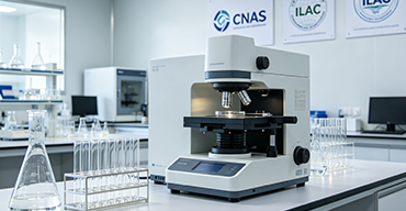
ZHONGXI Testing has obtained inspection qualification certifications from multiple countries and regions worldwide. We possess a senior testing team and advanced testing methods, providing independent, impartial, and professional third-party verification services for global carbon projects.
Internationally recognized authority
Certified by multiple international standards such as CNAS, VCS, and GS, with reports universally applicable worldwide.

Global service capability
Covering 140+ countries and regions, it supports on-site detection and remote verification in multiple languages.

Professional experimental methods
Adopt standard experimental methods to ensure accurate and reliable data.
Comprehensive Characterization of Molybdenum-Doped Indium Oxide (IMO) Thin Films – Advanced Analytical Services for Transparent Conductive Oxides
Molybdenum-doped indium oxide (IMO) thin films have emerged as a promising alternative to conventional indium tin oxide (ITO) in transparent conductive oxide (TCO) applications, offering tunable electrical conductivity, high optical transmittance, and improved work function stability. These films are increasingly employed in touch screens, flat-panel displays, organic light-emitting diodes (OLEDs), perovskite solar cells, and smart windows. However, the performance of IMO films is critically dependent on the molybdenum doping concentration, deposition parameters, post-deposition annealing, and film microstructure. A slight deviation in any of these factors can lead to reduced carrier mobility, increased resistivity, optical haze, or poor interfacial contact. Clients seeking IMO thin film testing services typically aim to: (i) verify the molybdenum content and its chemical state, (ii) measure electrical properties such as resistivity, carrier concentration, and Hall mobility, (iii) quantify optical transmittance, bandgap, and refractive index, (iv) assess crystalline quality, surface morphology, and film thickness, and (v) correlate these properties with deposition conditions to optimize process windows. Our laboratory offers a fully integrated, ISO/IEC 17025‑accredited IMO thin film characterization service that combines structural, electrical, optical, chemical, and morphological analysis into a unified platform. We do not merely report parameters; we deliver a correlative structure‑property‑performance picture that links doping chemistry, growth kinetics, and device performance, enabling our clients to accelerate development, reduce defects, and achieve competitive advantage in the TCO market.
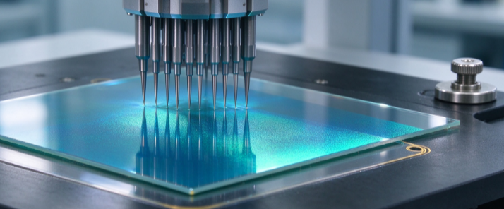
Why Professional IMO Thin Film Testing Is Essential for Device Performance and Reliability
IMO films are complex multicomponent oxides whose properties are highly sensitive to deposition and processing. The incorporation of molybdenum into the In₂O₃ lattice can substitute for indium, create oxygen vacancies, or form secondary phases depending on the doping level and oxygen partial pressure during deposition. These changes directly affect the free carrier concentration, optical absorption edge, and work function. Without rigorous characterization, these effects remain hidden until device fabrication, resulting in low yield, poor efficiency, or premature failure. Our testing services provide the objective evidence needed to diagnose process drift, qualify new suppliers, and support technology transfer. We help clients navigate the complex landscape of standards and specifications, including ASTM F1249, F1711, ISO 14707, and SEMI M1, ensuring that every IMO film meets the stringent requirements of its intended application.
Structural and Crystallographic Analysis – XRD, TEM, and Raman Spectroscopy
The crystalline quality and phase purity of IMO thin films directly influence carrier transport and optical properties. Our primary technique is high‑resolution X‑ray diffraction (HR‑XRD) (PANalytical X'Pert MRD) with a four‑crystal monochromator and a triple‑axis analyzer. We perform ω‑2θ scans to identify the cubic bixbyite In₂O₃ phase and detect any secondary phases such as MoO₃ or In₂Mo₃O₁₂. We determine the lattice parameter, crystallite size using the Scherrer equation, and microstrain via Williamson‑Hall analysis. Rocking curve (ω‑scan) measurements on the (222) or (400) reflection provide the mosaic spread and a quantitative measure of crystalline perfection. For nanoscale structural analysis, we use transmission electron microscopy (TEM) (JEOL JEM‑2100F) on cross‑sectional lamellae prepared by focused ion beam (FIB). High‑resolution TEM (HRTEM) reveals atomic‑scale interface abruptness, grain boundaries, and the presence of Mo‑rich clusters or precipitates. Selected area electron diffraction (SAED) confirms phase identity and epitaxial relationships. We complement XRD and TEM with Raman spectroscopy (Horiba LabRAM HR Evolution) using a 532 nm laser to detect the characteristic In₂O₃ phonon modes, which are sensitive to doping, strain, and oxygen vacancies.
Electrical Properties – Hall Effect, Resistivity, and Carrier Transport
The electrical performance of IMO films is the primary reason for their selection as TCOs. We perform room‑temperature and temperature‑dependent Hall effect measurements (van der Pauw geometry) with a magnetic field up to 1.5 T, extracting sheet resistance, carrier concentration (n‑type), and Hall mobility. For high‑resistivity films, we use a high‑impedance electrometer and guard‑ring configurations to minimize leakage. We also perform capacitance‑voltage (C‑V) measurements on Schottky or MIS structures to determine the built‑in potential, depletion width, and interface trap density (Dit). For doping profiling, we use electrochemical capacitance‑voltage (ECV) profiling, which provides depth‑resolved carrier concentration without the need for destructive sample preparation. We also assess photoconductivity under AM1.5 illumination to evaluate the film’s response to light, including gain, responsivity, and response time. For large‑area uniformity, we use a four‑point probe mapping system with a spatial resolution of 1 mm, ensuring consistent performance across the film.
Optical Properties – Transmittance, Bandgap, and Refractive Index
The optical performance of IMO films is critical for transparent electrode applications, where high transmittance in the visible and near‑infrared is required to maximize light transmission. Our primary tool is a UV‑Vis‑NIR spectrophotometer (PerkinElmer Lambda 950) with an integrating sphere for absolute transmittance and reflectance measurements from 200 nm to 2500 nm. We derive the absorption coefficient (α) and determine the optical bandgap (Eg) using Tauc plots for direct and indirect transitions, with an accuracy of ±0.01 eV. We also measure refractive index (n) and extinction coefficient (k) by spectroscopic ellipsometry (J.A. Woollam RC2‑XI) across 190–1700 nm, providing the data needed for optical modeling and device simulation. For haze and clarity, we use a hazemeter (ASTM D1003) and a laser‑based distortion system. We also assess color using CIE L*a*b* coordinates and chromaticity difference (ΔE*) to ensure batch‑to‑batch consistency.
Compositional and Surface Analysis – XPS, SIMS, and Auger Electron Spectroscopy
Accurate determination of molybdenum content and its chemical state is essential for controlling the electrical and optical properties of IMO films. Our X‑ray photoelectron spectroscopy (XPS) (Thermo Scientific K‑Alpha) with monochromated Al Kα radiation and in‑situ argon ion sputtering provides depth profiling of In, Mo, O, C, and other elements. We quantify the Mo:In ratio, detect oxide formation (MoO₃, MoO₂), and identify surface contamination. For trace impurities and dopant profiling, we use secondary ion mass spectrometry (SIMS) (Cameca IMS 7f) with both O₂⁺ and Cs⁺ primary beams, achieving detection limits down to 1×10¹⁵ atoms/cm³ for transition metals and 1×10¹⁸ atoms/cm³ for O and C. We also perform Auger electron spectroscopy (AES) depth profiling for lighter elements and high‑spatial‑resolution chemical mapping. For bulk composition, we use Rutherford backscattering spectrometry (RBS) with 2 MeV He⁺ ions, providing areal density and depth profiles without matrix effects. All chemical data are correlated with electrical measurements to identify compensation mechanisms and to guide deposition optimization.
Morphological and Thickness Measurements – AFM, SEM, and Ellipsometry
The surface morphology and thickness of IMO thin films affect light scattering, interface quality, and subsequent layer deposition. We employ atomic force microscopy (AFM) (Bruker Dimension FastScan) in tapping mode to measure surface roughness (Ra, Rq, Rz) over scan areas from 1 μm × 1 μm to 50 μm × 50 μm. We provide statistical parameters and power spectral density (PSD) curves that fingerprint the growth mode and reveal pinholes, hillocks, or grain structure. For wide‑area inspection, we use a field‑emission scanning electron microscope (FE‑SEM) (FEI Verios 460) with automated defect classification, enabling the detection of particles, cracks, and delamination. Film thickness is determined by spectroscopic ellipsometry (SE) and X‑ray reflectivity (XRR), with sub‑nanometer precision for films ranging from 5 nm to 500 nm. We also use profilometry and cross‑sectional SEM for direct thickness verification. For conformality and step coverage, we examine films deposited on patterned substrates using FIB‑SEM cross‑sections.
Advanced Defect and Interface Analysis – DLTS, EBIC, and CL Mapping
Deep‑level defects and interface states are often the limiting factors in IMO‑based devices. We perform deep‑level transient spectroscopy (DLTS) on Schottky diodes or heterojunctions to identify trap levels with activation energies, capture cross‑sections, and concentrations. This is particularly valuable for detecting oxygen‑vacancy‑related defects, molybdenum clusters, or stress‑induced traps. We also use electron‑beam‑induced current (EBIC) in a SEM to map the minority carrier diffusion length and locate recombination centers at grain boundaries or interfaces. Cathodoluminescence (CL) mapping at low temperature provides spatial resolution of radiative and non‑radiative defects, revealing inhomogeneities that are invisible in ensemble measurements. For interface analysis, we combine TEM‑EDS and electron energy loss spectroscopy (EELS) to quantify interdiffusion and chemical bonding at the IMO/absorber interface, which is critical for device efficiency and stability.
Our Distinctive Competencies – Integrated Platform, Expert Team, and Rapid Turnaround
What sets our IMO thin film testing service apart is the seamless integration of structural, electrical, optical, chemical, and morphological characterization within a single laboratory, enabling correlative analysis that is impossible when samples are shipped between multiple vendors. Our team comprises PhD‑level materials scientists, physicists, and engineers with extensive experience in transparent conductive oxides, thin‑film deposition, and device physics. We do not simply report numbers; we interpret them in terms of deposition chemistry, growth kinetics, and device performance – for example, distinguishing between resistivity changes caused by carrier concentration versus mobility, or identifying the root cause of optical haze as surface roughness versus bulk defects.
Our laboratory is ISO/IEC 17025 accredited for many of the key test methods (XRD, XPS, SIMS, Hall, UV‑Vis, AFM), and we maintain NIST‑traceable calibrations for all equipment. We participate in international round‑robins (e.g., VAMAS, ASTM) to ensure global comparability. We offer rapid turnaround – typically 3–5 business days for a standard characterization package – and we accept samples in various forms: thin films on glass, silicon, or flexible substrates; full wafers; and small coupons. Our data analytics platform employs machine learning to identify subtle correlations between deposition parameters and film properties, accelerating process optimization.
We also provide custom test plans for emerging IMO‑based materials (e.g., co‑doped In₂O₃, amorphous IMO, and multilayer stacks) and for non‑standard device architectures (e.g., flexible electronics, perovskite tandem cells). Our consulting services include interpretation of results, design of experiments (DoE) for process improvement, and troubleshooting of deposition defects.
Comprehensive Service Modules – Tailored to Your IMO Film Requirements
We offer a modular testing structure that allows clients to select the exact measurements needed for their specific IMO thin film:
Module 1 – Structural and Phase Analysis: HR‑XRD, Raman, and TEM for crystallinity, phase purity, and texture – essential for deposition quality control.
Module 2 – Electrical Properties: Hall effect, resistivity, C‑V, ECV, and four‑point probe mapping – for carrier concentration, mobility, and uniformity.
Module 3 – Optical Properties: Transmittance, bandgap, ellipsometry, haze, and color – for transparent electrode optimization.
Module 4 – Compositional and Surface Analysis: XPS, SIMS, RBS, and AES for stoichiometry, Mo content, and interface chemistry.
Module 5 – Morphology and Thickness: AFM, SEM, ellipsometry, and XRR for roughness, thickness, and defect density.
Module 6 – Advanced Defect and Interface Analysis: DLTS, EBIC, CL mapping, and TEM‑EELS for trap identification and interface quality.
Module 7 – Comprehensive IMO Qualification Package: All modules combined, plus a final integrated report with correlations, statistical analysis, and expert recommendations – suitable for technology transfer, supplier qualification, or regulatory submission.
We also design custom test plans for special requirements, such as temperature‑dependent Hall up to 500 K, high‑resolution XRD for ultrathin layers, or polarization‑resolved PL.
Data Integrity, Security, and Reporting
All measurements are performed under strictly controlled conditions (class 100 cleanroom for sensitive samples), with NIST‑traceable calibrations and comprehensive SOPs. Our Laboratory Information Management System (LIMS) records every operation, operator, and environmental parameter, ensuring full auditability. We adhere to strict confidentiality protocols – all client data are encrypted, access‑controlled, and retained securely. We provide comprehensive reports with tables, graphs, uncertainty statements, and an executive summary that translates technical findings into actionable business insights. Raw data files are available upon request. A post‑delivery review meeting is included to discuss results and recommend next steps.
Client Engagement and Workflow
Our engagement begins with a complimentary consultation to understand your IMO film type, deposition method, intended application, and specific concerns (e.g., resistivity, transmittance, or doping uniformity). We then propose a tailored test plan with a fixed price and timeline. Upon sample receipt, we log and inspect the samples, then commence testing. Clients receive progressive updates through a secure portal, with preliminary data shared on request. The final report is delivered in PDF format, and we offer a follow‑up call to discuss the findings and their implications for your development or production.
Conclusion – Empowering Your IMO Thin Film Technology with Unmatched Analytical Depth
Molybdenum-doped indium oxide thin films are enabling the next generation of transparent electrodes for displays, solar cells, and smart windows, but their full potential can only be realized through rigorous, multidimensional, and physics‑based characterization. Our comprehensive, ISO‑accredited testing service provides exactly that – a one‑stop solution that combines structural, electrical, optical, chemical, and morphological analyses into a unified, interpretable picture. With our advanced instrumentation, deep materials expertise, and collaborative approach, we empower our clients to accelerate development, reduce defects, and confidently bring high‑quality IMO‑based devices to market.
We invite you to contact our IMO thin film characterization specialists to discuss your specific testing needs. Let us partner with you to ensure that your IMO layers meet the highest standards of quality and performance – from the deposition chamber to the final device. Your journey to IMO thin film excellence begins with our rigorous, integrative, and actionable testing.