Reasons for choosing our testing services
ZHONGXI Testing has obtained inspection qualification certifications from multiple countries and regions worldwide. We possess a senior testing team and advanced testing methods, providing independent, impartial, and professional third-party verification services for global carbon projects.

Internationally recognized authority
Certified by multiple international standards such as CNAS, VCS, and GS, with reports universally applicable worldwide.

Global service capability
Covering 140+ countries and regions, it supports on-site detection and remote verification in multiple languages.

Professional experimental methods
Adopt standard experimental methods to ensure accurate and reliable data.
Advanced Photomask Inspection and Metrology Services – Ensuring Lithographic Excellence from Design to Wafer
Photomasks are the master templates that transfer circuit patterns onto semiconductor wafers, flat panel displays, and micro‑optical devices. A single undetected defect, critical dimension (CD) deviation, registration error, or phase‑shift anomaly can propagate through millions of exposure cycles, causing yield loss, device failure, and costly downtime. Clients seeking photomask inspection services typically aim to: (i) qualify new mask sets before committing to wafer production, (ii) monitor mask quality during long production runs, (iii) verify repair success after defect mitigation, (iv) assess flatness and pellicle integrity for overlay and focus control, and (v) generate certification data for mask shops, foundries, and OEM audits. Our laboratory offers a fully integrated, ISO/IEC 17025‑accredited photomask inspection and metrology service that combines optical and DUV defect inspection, e‑beam review, CD‑SEM, AFM, spectroscopic ellipsometry, phase metrology, registration measurement, flatness characterization, and actinic review into a unified assessment platform. We do not merely report pass/fail results; we deliver a holistic mask quality fingerprint that correlates pattern fidelity, material properties, and environmental stability with wafer‑level performance, empowering our clients to accelerate mask qualification, reduce lithography risk, and achieve advanced‑node yield targets.
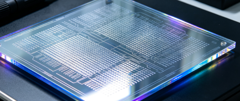
Why Professional Photomask Inspection Is Indispensable for Lithography Yield and Device Performance
Photomasks are used repeatedly under intense DUV or EUV illumination, thermal cycling, and mechanical handling. Over time, they can accumulate particles, haze, pellicle degradation, and pattern wear. Even a sub‑100 nm defect can print as a killer defect on the wafer, especially at advanced nodes where the mask error enhancement factor (MEEF) amplifies small deviations. Moreover, aggressive optical proximity correction (OPC), phase‑shifting structures, and sub‑resolution assist features (SRAFs) make masks highly complex and sensitive to process variations. Regulatory and industry standards such as SEMI P1, P35, P37, P38, and ISO 14644 impose strict requirements on defect density, CD uniformity, registration accuracy, and flatness. Our testing services provide the objective evidence needed to qualify mask suppliers, monitor degradation, and support technology transfer. We help clients navigate the complex landscape of mask specifications, ensuring that every photomask meets the stringent requirements of its intended lithography process.
Comprehensive Defect Inspection – Optical, DUV, E‑Beam, and Actinic Review
Defect inspection is the cornerstone of photomask quality control. Our platform includes deep‑ultraviolet (DUV) laser scanning inspection at 193 nm and 248 nm, capable of detecting defects down to 20 nm in both die‑to‑die and die‑to‑database modes. We also employ high‑resolution optical inspection with confocal and bright‑field/dark‑field imaging for pattern fidelity and particle detection. For critical defects, we perform e‑beam review using a scanning electron microscope (SEM) with automated defect classification (ADC) based on machine‑learning algorithms, which distinguish between particles, pits, scratches, pattern defects, and phase errors. Actinic inspection at 193 nm or 13.5 nm (EUV) provides the highest sensitivity for phase‑shift and EUV masks, revealing defects that may not be visible with conventional optical methods. Our atomic force microscopy (AFM) provides three‑dimensional metrology of defect geometry, including depth, width, and sidewall angle, enabling precise repair planning. We also offer mask blank inspection for substrate pits, scratches, and multilayer defects before patterning, which is critical for EUV masks.
Critical Dimension, Registration, and Pattern Fidelity Metrology
Critical dimension (CD) uniformity and registration accuracy are essential for overlay and device performance. Our CD‑SEM systems measure linewidth, space width, and pitch with sub‑nanometer precision across the entire mask, generating 2D CD uniformity maps with a spatial resolution of 1 mm. We also use scatterometry and spectroscopic ellipsometry for non‑destructive CD and profile measurement on production masks. Registration metrology is performed using a laser interferometric stage with a coordinate accuracy of better than 1 nm, measuring pattern placement errors (PPE) and overlay. We also assess image placement and pattern fidelity by comparing the mask design to the fabricated pattern using die‑to‑database inspection and CD‑SEM contour extraction. For advanced OPC and SRAFs, we perform aerial image simulation and through‑focus CD analysis to predict wafer‑level process windows. Our reports include CD uniformity maps, registration vectors, and MEEF analysis, providing actionable data for mask makers and lithography engineers.
Phase, Transmission, and Material Property Characterization
Phase‑shift masks (PSMs) and EUV masks require precise control of phase and transmission. We measure phase shift using a phase‑measuring interferometer or spectroscopic ellipsometry with an accuracy of ±0.5° at 193 nm or 13.5 nm. Transmission is measured by spectrophotometry from 150 nm to 800 nm, including the effects of absorber stack, capping layers, and pellicle. We also characterize refractive index (n) and extinction coefficient (k) of mask materials (MoSi, TaBN, etc.) using ellipsometry, providing data for optical proximity correction and simulation. Film thickness and composition are measured by X‑ray reflectivity (XRR), X‑ray photoelectron spectroscopy (XPS), and secondary ion mass spectrometry (SIMS). For EUV masks, we assess multilayer periodicity, interface roughness, and defect density using grazing‑incidence X‑ray diffraction and TEM. Our laboratory also offers contamination analysis for haze, ionic residues, and organics using time‑of‑flight SIMS (ToF‑SIMS) and ion chromatography.
Flatness, Surface Quality, and Pellicle Integrity Assessment
Mask flatness directly affects overlay, focus, and pattern placement. We measure flatness, bow, and warp using a laser interferometer or capacitance probe system with sub‑100 nm accuracy, generating full‑mask topography maps. Surface roughness is measured by AFM over scan areas from 1 μm × 1 μm to 100 μm × 100 μm, providing Ra, Rq, and Rz values. We also inspect for scratches, pits, and particles using dark‑field optical microscopy and SEM. For masks with pellicles, we evaluate pellicle transmission, haze growth, and adhesion under accelerated aging conditions (e.g., 193 nm irradiation, humidity, and thermal cycling). We also measure pellicle flatness and gap uniformity, which affect focus and aberration. Our reports include flatness contour maps, roughness statistics, and pellicle degradation rates, enabling clients to optimize mask handling and storage.
EUV and Advanced Mask Technologies
EUV lithography introduces unique challenges for mask inspection. EUV masks are reflective, consisting of a multilayer Mo/Si stack, a TaBN absorber, and a capping layer. Defects can occur in the multilayer, at the absorber, or on the surface. Our laboratory offers EUV mask blank inspection using actinic dark‑field imaging at 13.5 nm, atomic force microscopy for surface defects, and X‑ray diffraction for multilayer periodicity. We also perform EUV mask pattern inspection using e‑beam review and actinic inspection to detect absorber defects, phase defects, and multilayer perturbations. For EUV masks with pellicles, we assess transmission loss and thermal stability under high‑power EUV exposure. We also offer mask 3D effect analysis using rigorous coupled‑wave analysis (RCWA) and finite‑difference time‑domain (FDTD) simulation, correlating mask topography with wafer‑level imaging performance. Our team has extensive experience with EUV mask infrastructure and can support clients from mask blank qualification to final mask acceptance.
Repair Verification and Post‑Repair Qualification
Mask repair is a critical step in extending mask life and reducing cost. After repair – whether by focused ion beam (FIB), electron‑beam induced deposition (EBID), or laser ablation – the repaired site must be verified to ensure that the defect is removed, the pattern fidelity is restored, and no new defects are introduced. Our repair verification service includes high‑resolution SEM review, AFM metrology of the repaired area, CD‑SEM measurement of the repaired feature, and aerial image simulation to predict wafer‑level impact. We also perform through‑focus CD analysis and process window qualification to ensure that the repair does not degrade lithographic performance. For phase‑shift masks, we verify phase and transmission at the repair site. Our reports include before/after images, CD measurements, and a clear pass/fail disposition with recommendations for re‑repair or mask rejection.
Reliability, Contamination, and Lifetime Assessment
Photomask reliability is critical for high‑volume manufacturing. We perform accelerated lifetime testing under DUV or EUV irradiation, thermal cycling, and humidity exposure, monitoring CD drift, transmission loss, haze growth, and registration stability. We also assess contamination resistance by exposing masks to controlled environments and measuring particle deposition, ionic contamination, and outgassing. Our laboratory offers haze analysis using scanning electron microscopy (SEM), energy‑dispersive X‑ray spectroscopy (EDS), and ion chromatography to identify the chemical composition of haze and its origin. We also perform mask cleaning validation to ensure that cleaning processes remove contaminants without damaging the pattern or altering the phase/transmission properties. Our reports include degradation rates, lifetime predictions, and recommendations for cleaning frequency and storage conditions.
Our Distinctive Competencies – Instrumentation, Expertise, and Accreditation
What sets our photomask inspection service apart is the seamless integration of defect inspection, CD metrology, registration, phase/transmission characterization, flatness measurement, and repair verification within a single laboratory, enabling correlative analysis that is impossible when samples are shipped between multiple vendors. Our team comprises PhD‑level physicists, materials scientists, and lithography engineers with extensive experience in mask technology, advanced nodes, and EUV infrastructure. We do not simply report numbers; we interpret them in terms of mask design, fabrication, and lithographic performance – for example, distinguishing between a CD error caused by e‑beam writing versus etch loading, or identifying the root cause of registration error as stage drift versus pattern placement error.
Our laboratory is ISO/IEC 17025 accredited for a wide range of photomask test methods, and we maintain NIST‑traceable calibrations for all equipment. We participate in international round‑robins (e.g., SEMI, NIST, PTB) to ensure global comparability. We offer rapid turnaround – typically 3–5 business days for standard inspection packages, with expedited options available – and we accept samples in various forms: 6‑inch and 9‑inch photomasks, EUV masks, and mask blanks. Our data analytics platform employs machine learning to identify subtle correlations between mask process parameters and defectivity, accelerating yield improvement and process optimization.
We also provide custom test plans for emerging mask technologies (e.g., EUV, nanoimprint, and curved masks) and for specific applications (e.g., logic, memory, display, and photonics). Our consulting services include mask specification review, supplier qualification, certification strategy, and failure analysis with root‑cause determination. We offer on‑site sampling and mobile inspection units for large‑scale mask shops and foundries, ensuring that critical measurements can be performed without transport delays.
Comprehensive Service Modules – Tailored to Your Mask Type and Application
We organize our testing into modular packages to meet diverse client objectives:
Module 1 – Defect Inspection and Review: DUV laser scanning, optical inspection, e‑beam review, actinic inspection, and AFM – for defect detection, classification, and disposition.
Module 2 – CD, Registration, and Pattern Fidelity: CD‑SEM, scatterometry, registration metrology, die‑to‑database inspection, and aerial image simulation – for critical dimension uniformity and overlay control.
Module 3 – Phase, Transmission, and Material Properties: Phase metrology, spectrophotometry, ellipsometry, XRR, XPS, and SIMS – for phase‑shift and EUV mask characterization.
Module 4 – Flatness, Surface Quality, and Pellicle Integrity: Laser interferometry, capacitance probe, AFM, pellicle transmission, and haze testing – for flatness, roughness, and pellicle reliability.
Module 5 – EUV and Advanced Mask Technologies: Actinic inspection, multilayer characterization, mask 3D effect analysis, and EUV pellicle testing – for next‑generation lithography.
Module 6 – Repair Verification and Post‑Repair Qualification: SEM review, AFM, CD‑SEM, aerial image simulation, and through‑focus CD analysis – for repair quality assurance.
Module 7 – Reliability, Contamination, and Lifetime Assessment: Accelerated lifetime testing, haze analysis, cleaning validation, and contamination resistance – for mask lifetime prediction.
Module 8 – Comprehensive Photomask Qualification Package: All modules combined into a single project, with integrated correlation analysis, statistical summary, and a detailed interpretive report – suitable for mask qualification, supplier audits, or regulatory submissions.
We also design custom test plans for special requirements, such as high‑resolution CD metrology for sub‑10 nm nodes, actinic inspection for EUV, or through‑pellicle inspection for production masks.
Data Integrity, Security, and Reporting
All measurements are performed under strict SOPs, with fully traceable calibration records and environmental logging. Our Laboratory Information Management System (LIMS) records every operation, operator, and timestamp, ensuring full auditability. We use encrypted data transfer and role‑based access to protect client proprietary information. Our reports include comprehensive tables, graphs, uncertainty statements, and an executive summary that translates technical findings into actionable insights. Raw data files are available upon request. A post‑delivery review meeting is included to discuss results and recommend next steps.
Client Engagement and Workflow
Our engagement begins with a complimentary consultation to understand your mask type, lithography node, intended application, and specific concerns (e.g., defect density, CD uniformity, or registration). We then propose a tailored test plan with a fixed price and timeline. Upon sample receipt, we log and inspect the samples, then commence testing. Clients receive progressive updates through a secure portal, with preliminary data shared on request. The final report is delivered in PDF format, and we offer a follow‑up call to discuss the findings and their implications for your mask qualification or production.
Conclusion – Ensuring Photomask Excellence from Design to Wafer
Photomasks are the master templates that determine the success of every lithographic process, and their reliable performance depends on rigorous, multidimensional testing that goes beyond simple visual inspection. Our comprehensive, ISO‑accredited testing service provides exactly that – a one‑stop solution that combines defect inspection, CD metrology, registration, phase/transmission characterization, flatness measurement, and repair verification into a unified, interpretable picture. With our advanced instrumentation, deep materials expertise, and collaborative approach, we empower our clients to accelerate mask qualification, reduce lithography risk, and confidently bring high‑quality photomasks to production. Whether you are developing EUV masks, phase‑shift masks, or advanced OPC masks, our service delivers the clarity and confidence you need to succeed.
We invite you to contact our photomask inspection specialists to discuss your specific requirements. Let us partner with you to ensure that your photomasks meet the highest standards of quality, fidelity, and reliability – from the mask shop to the wafer fab. Your journey to photomask excellence begins with our rigorous, integrative, and actionable testing.