Reasons for choosing our testing services
ZHONGXI Testing has obtained inspection qualification certifications from multiple countries and regions worldwide. We possess a senior testing team and advanced testing methods, providing independent, impartial, and professional third-party verification services for global carbon projects.

Internationally recognized authority
Certified by multiple international standards such as CNAS, VCS, and GS, with reports universally applicable worldwide.

Global service capability
Covering 140+ countries and regions, it supports on-site detection and remote verification in multiple languages.

Professional experimental methods
Adopt standard experimental methods to ensure accurate and reliable data.
Epitaxial Substrate Inspection Services for Epitaxy-Ready Wafer Qualification and Yield Control
Customers searching for epitaxial substrate inspection typically need to qualify incoming material, benchmark suppliers, control polishing and cleaning processes, predict epitaxial growth behavior, and prevent substrate defects from propagating into device layers. Our service is designed for exactly this purpose. We provide quantitative, application-relevant inspection of substrates used for epitaxy so that customers can make confident engineering, qualification, and production decisions.
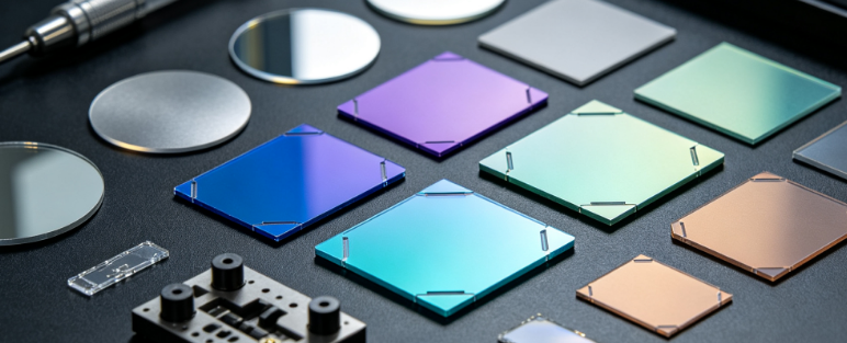
Why Epitaxial Substrate Inspection Is Requested
Epitaxial growth is highly sensitive to substrate geometry, surface finish, crystallographic perfection, contamination, and near-surface damage. A substrate that appears acceptable by basic visual inspection may still produce haze, pits, stacking faults, threading dislocations, poor nucleation, or non-uniform doping during epitaxy. Our epitaxial substrate inspection service helps customers detect these risks before epitaxial growth, correlate substrate quality with process conditions, and establish objective acceptance criteria for incoming and outgoing wafers.
Typical customer objectives include incoming quality control, supplier qualification, process development, epitaxy-ready release, failure analysis, and yield improvement. We support these objectives with a customizable inspection workflow that combines non-destructive screening, high-resolution metrology, and targeted destructive analysis.
Substrate Types and Inspection Scope We Support
We inspect epitaxial substrates including sapphire, silicon, 4H-SiC, GaN, GaAs, InP, Ga2O3, and other compound semiconductor materials. Substrate sizes from 2-inch to 12-inch are supported, including C-plane, R-plane, A-plane, M-plane, off-axis, and patterned sapphire substrates. We can evaluate full wafers, coupon samples, and production lots with wafer-level mapping, statistical analysis, and defect classification suitable for research, pilot lines, and high-volume manufacturing.
Geometry, Flatness, and Nanotopography Inspection
Geometric quality directly affects epitaxial uniformity, photolithography, bonding, and device reliability. We measure total thickness variation, bow, warp, local thickness variation, site total indicated reading, flatness, edge exclusion, and surface roughness. Using white-light interferometry, atomic force microscopy, laser scattering, and stylus profilometry, we characterize scratches, pits, particles, micro-cracks, edge chips, polishing marks, and step-height features. Our inspection supports sub-nanometer surface roughness resolution, angstrom-level step-height measurement, and full-wafer defect mapping with high spatial resolution.
Crystallographic and Structural Quality Assessment
Crystallographic perfection is critical for epitaxial layer quality. We employ high-resolution X-ray diffraction, reciprocal space mapping, Raman spectroscopy, electron backscatter diffraction, and transmission electron microscopy to evaluate lattice orientation, off-cut angle, mosaic tilt and twist, lattice strain, curvature, dislocations, stacking faults, twins, inclusions, and micropipes. Our capabilities include arcsecond-level misorientation measurement, ppm-level strain sensitivity, and quantitative dislocation density mapping. This depth of analysis allows customers to distinguish intrinsic substrate quality from process-induced damage and epitaxial growth issues.
Surface Chemistry, Contamination, and Epitaxial Readiness
Surface chemistry can influence nucleation, adhesion, and defect formation during epitaxy. We use X-ray photoelectron spectroscopy, total reflection X-ray fluorescence, secondary ion mass spectrometry, time-of-flight secondary ion mass spectrometry, Auger electron spectroscopy, spectroscopic ellipsometry, and photoluminescence to assess metallic contamination, organic residue, native oxide, surface termination, haze, and optical quality. We correlate surface chemistry, nanoscale topography, and crystallographic data to assess epitaxial readiness and to identify contamination sources that may cause poor layer quality or device failure.
Electrical and Optical Characterization
For conductive and semi-insulating substrates, electrical properties can affect device performance and process stability. We provide Hall effect measurements, capacitance-voltage profiling, mercury probe analysis, sheet resistance mapping, resistivity mapping, carrier concentration, mobility, and doping uniformity assessment. Optical characterization includes photoluminescence, Raman spectroscopy, UV-Vis spectroscopy, reflectance, and ellipsometry. We can map electrical and optical uniformity across the wafer and correlate these properties with structural and surface quality.
Destructive and Correlative Failure Analysis
Not every substrate defect can be resolved with surface-sensitive techniques alone. For root-cause analysis, we provide focused ion beam sample preparation, cross-sectional transmission electron microscopy, defect delineation etching, etch pit density analysis, and scanning electron microscopy with energy-dispersive X-ray spectroscopy. We integrate non-destructive screening with targeted destructive analysis so that customers receive both high-throughput process monitoring and high-confidence failure analysis. This combined approach is especially valuable for qualifying new polishing slurries, cleaning recipes, epitaxial processes, and supplier lots.
Data Reporting, Statistical Process Control, and Wafer Mapping
Our deliverables are designed for engineering and quality teams. Reports can include full-wafer defect maps, roughness maps, crystallographic orientation maps, thickness and flatness maps, defect Pareto charts, statistical process control trends, and root-cause hypotheses. We provide actionable data with traceable calibration protocols and clear pass or fail criteria based on relevant SEMI and industry standards. When required, we also support correlative failure analysis to link substrate defects with epitaxial or device-level failures.
Our Advantages in Epitaxial Substrate Inspection
Our core advantage is the ability to combine multiple high-end metrology platforms within one coordinated workflow. We bring together HRXRD, reciprocal space mapping, Raman, AFM, SEM/EDS, TEM, FIB, white-light interferometry, laser scattering, spectroscopic ellipsometry, photoluminescence, XPS, TXRF, SIMS, and electrical characterization. We do not merely detect defects; we quantify them, map them, classify them, and relate them to epitaxial growth and device performance. Our team supports custom inspection protocols, fast turnaround, confidential sample handling, and scalable programs for R&D, pilot lines, and high-volume manufacturing.
Applications and Industries We Support
Our epitaxial substrate inspection services support LED epitaxy, laser diodes, GaN high-electron-mobility transistors, radio-frequency devices, power electronics, photonic integrated circuits, sensors, and advanced research. We serve substrate suppliers, epitaxial wafer manufacturers, device fabs, and research institutions that require rigorous material characterization. Whether the goal is incoming quality control, supplier benchmarking, process development, or failure analysis, we provide the depth of inspection needed to make defensible technical decisions.
Request Epitaxial Substrate Inspection
To begin, customers can provide substrate type, size, orientation, surface finish, suspected defect types, and the intended epitaxial or device application. Based on these inputs, we design a targeted inspection plan that balances non-destructive screening, high-resolution analysis, and statistical reporting. We can build a customized epitaxial substrate inspection program that meets demanding technical specifications and production timelines. Contact us to discuss sample submission, measurement resolution, reporting format, and turnaround requirements.