Reasons for choosing our testing services
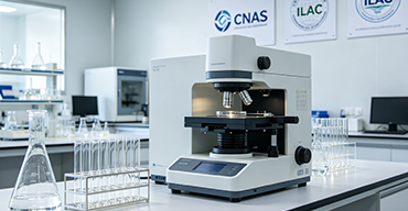
ZHONGXI Testing has obtained inspection qualification certifications from multiple countries and regions worldwide. We possess a senior testing team and advanced testing methods, providing independent, impartial, and professional third-party verification services for global carbon projects.
Internationally recognized authority
Certified by multiple international standards such as CNAS, VCS, and GS, with reports universally applicable worldwide.

Global service capability
Covering 140+ countries and regions, it supports on-site detection and remote verification in multiple languages.

Professional experimental methods
Adopt standard experimental methods to ensure accurate and reliable data.
Crystalline Silicon Solar Cell Surface Oxidation Detection: Advanced Characterisation for Efficiency Optimisation and Reliability Assurance
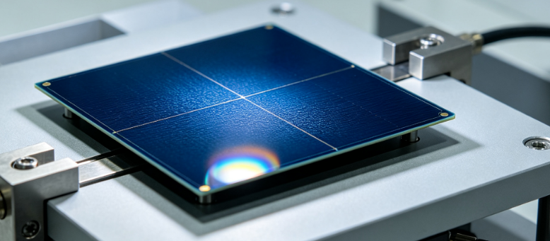
Surface oxidation on crystalline silicon solar cells—whether in the form of native oxide layers, thermally grown SiO₂, or chemically induced sub‑oxides—critically influences photovoltaic performance, particularly through recombination losses, contact resistance, and light‑trapping effects. A thin oxide layer of just 0.5 nm can alter the surface passivation quality and the effective minority carrier lifetime, while non‑uniform oxidation can lead to localised shunting or degraded blue‑light response. Standard quality control methods such as simple ellipsometry at a single wavelength or qualitative X‑ray photoelectron spectroscopy (XPS) often fail to capture the full chemical complexity, sub‑nanometre thickness variations, and spatial heterogeneity of the oxide. Our detection service is specifically designed to deliver a multi‑technique, quantitative, and spatially resolved characterisation of oxide layers on crystalline silicon wafers and finished cells, covering thickness, chemical composition (stoichiometry), surface coverage, and the presence of carbonaceous or metallic contaminants. We employ state‑of‑the‑art spectroscopic ellipsometry, high‑resolution XPS with depth profiling, micro‑Raman imaging, and Fourier‑transform infrared (FTIR) spectroscopy to provide absolute oxide thickness with ±0.02 nm accuracy, detailed sub‑oxide (SiOx) stoichiometry, and 2D distribution maps across the entire wafer surface. These data enable manufacturers, R&D teams, and quality assurance laboratories to fine‑tune cleaning and passivation processes, diagnose efficiency losses, predict long‑term stability, and ensure compliance with stringent industry standards.
Why Specialised Surface Oxidation Testing Is Essential for Solar Cell Performance and Durability
The oxide layer on silicon is not a simple, homogeneous SiO₂ film; it often contains intermediate oxidation states (Si¹⁺, Si²⁺, Si³⁺), hydroxyl groups, and adsorbed organic species that can act as recombination centres or affect the subsequent deposition of antireflective coatings and metal contacts. Even a 0.3 nm variation in oxide thickness across a 156 mm wafer can cause a 2–3% relative efficiency drop due to non‑uniform reflectance. Moreover, the oxide layer is continuously evolving during processing and storage—exposure to light, humidity, and elevated temperatures can induce further oxidation or contaminant adsorption, leading to gradual performance degradation (light‑induced degradation, PID). Routine inspection based on visual appearance or contact angle measurement is insufficient; our testing protocols are designed to quantify the oxide's physical and chemical properties at the atomic scale, enabling root‑cause analysis of poor cell performance, optimisation of wet‑chemical cleaning and passivation steps, and verification of the effectiveness of anti‑reflective coatings.
Our Core Detection Capabilities for Crystalline Silicon Surface Oxidation
We operate a dedicated solar cell characterisation laboratory, equipped with advanced optical and surface analytical instruments, all calibrated against NIST‑traceable standards. The following represent our standard high‑end offerings:
Spectroscopic Ellipsometry (SE) with Multi‑Wavelength and In‑Situ Mapping: We use a variable‑angle spectroscopic ellipsometer (range 190–2500 nm, with rotating compensator) to determine the thickness, refractive index (n), and extinction coefficient (k) of the oxide layer and any underlying or overlying films. By measuring at multiple angles (55°–80°) and fitting the data with a multi‑oscillator model (Tauc‑Lorentz or Cody‑Lorentz for the silicon substrate, and a Cauchy or oscillator model for the oxide), we extract the oxide thickness with a precision of ±0.02 nm and the surface roughness with ±0.1 nm accuracy. We perform mapping ellipsometry (with a 2D stage, step size 2 mm) to generate thickness uniformity maps of the entire wafer surface, revealing any radial or edge‑induced variations. Our models also distinguish between stoichiometric SiO₂ and silicon‑rich sub‑oxides by analysing the spectral dispersion in the UV region.
High‑Resolution X‑Ray Photoelectron Spectroscopy (XPS) with Angle‑Resolved and Depth Profiling: Our monochromatic Al Kα XPS system (spot size 10 µm, energy resolution 0.3 eV) provides chemical state analysis of silicon, oxygen, and any contaminants (carbon, nitrogen, metals). We collect high‑resolution Si 2p spectra and perform peak decomposition to quantify the relative amounts of Si0 (bulk silicon), Si1+, Si2+, Si3+, and Si4+ (SiO₂) species. From this, we derive the average oxide stoichiometry (x in SiOx) and the sub‑oxide thickness. Using angle‑resolved XPS (ARXPS) at multiple take‑off angles, we perform non‑destructive depth profiling of the oxide (0–10 nm) to reveal the transition region between the bulk silicon and the native oxide. For deeper profiles, we use low‑energy Ar⁺ cluster sputtering to obtain concentration vs. depth profiles with a depth resolution of ~0.5 nm, quantifying the oxide thickness and the interface roughness. We also detect trace contaminants (e.g., Na, K, Fe) at sub‑ppm levels that may induce surface recombination.
Micro‑Raman Spectroscopy for Stress and Phase Mapping: We use a confocal Raman microscope (excitation 325, 532, and 785 nm) with a spatial resolution of 0.5 µm to map the crystalline silicon phonon peak (520 cm⁻¹) and the oxide‑related peaks (∼440–520 cm⁻¹ for sub‑oxides, and 800–1200 cm⁻¹ for SiO₂). The Raman shift provides information on residual stress in the oxide and the silicon substrate, which can arise from thermal or mechanical processing and affect device reliability. We generate stress distribution maps that reveal any localised strain fields due to non‑uniform oxidation or contact formation.
Fourier‑Transform Infrared Spectroscopy (FTIR) in ATR and Transmission Modes: We perform transmission FTIR on double‑sided polished wafers to measure the Si‑O‑Si stretching (∼1100 cm⁻¹) and bending (∼800 cm⁻¹) vibrations, providing a bulk‑averaged oxide thickness and the concentration of silanol (Si‑OH) groups (∼3650 cm⁻¹) that indicate incomplete oxidation or humidity absorption. For non‑polished cells, we use attenuated total reflectance (ATR) with a germanium crystal to obtain surface‑sensitive spectra. The integrated absorbance of the Si‑O peak is calibrated against ellipsometric thickness, achieving a thickness accuracy of ±0.05 nm for thin oxides.
Atomic Force Microscopy (AFM) for Surface Topography and Oxide Distribution: We use a tapping‑mode AFM with a sharp tip (radius < 5 nm) to image the surface roughness at the nanoscale and to detect any pinholes or localised thick oxide islands. We provide roughness parameters (Sa, Sq, Sz) and power spectral density (PSD) to characterise the spatial frequency of surface features. For selected areas, we perform nanoscale electrical characterisation (conductive AFM) to correlate surface oxide thickness with local current leakage.
Secondary Ion Mass Spectrometry (SIMS) for Trace Impurity and Isotopic Analysis: For ultra‑trace detection of dopants and contaminants in the oxide, we employ dynamic SIMS with a Cs⁺ or O₂⁺ primary beam, achieving a detection limit of 10¹⁴ atoms/cm³ for elements like B, P, Na, and Fe. We provide depth profiles of oxygen, hydrogen, carbon, and metal impurities, which are critical for assessing the cleanliness of wet‑chemical processes and the effectiveness of passivation.
Minority Carrier Lifetime Measurement (Quasi‑Steady‑State Photoconductance – QSSPC): We use a Sinton Instruments WCT‑120 to measure the effective minority carrier lifetime (τeff) of the silicon wafer before and after oxide formation. By correlating the lifetime with the oxide thickness and stoichiometry (from ellipsometry/XPS), we identify the optimal oxide passivation quality and the surface recombination velocity (SRV) attributable to the oxide. This is a direct link between oxide characterisation and cell performance.
Accelerated Ageing and Environmental Stability Tests: We expose the oxidised wafers to damp heat (85 °C/85% RH), UV irradiation (with and without humidity), and thermal cycling (−40 °C to +85 °C) for up to 1000 hours, and we re‑characterise the oxide thickness and composition. We quantify the oxide growth rate and the formation of new sub‑oxide species under stress, providing a prediction of long‑term stability and the risk of light‑induced degradation (LID) or potential‑induced degradation (PID).
Integrated Analytical Framework: Cross‑Correlation of Optical, Chemical, and Electrical Data
Our unique strength lies in the systematic correlation of ellipsometric thickness, XPS sub‑oxide ratio, FTIR absorbance, and lifetime measurements. Using our proprietary software (OxideProfiler™), we build a comprehensive oxide quality index that combines thickness uniformity, stoichiometry, interface roughness, and recombination activity into a single figure of merit. This index is used to compare different oxidation processes (thermal, UV‑ozone, plasma‑assisted) and to track batch‑to‑batch consistency. We also provide multivariate analysis to identify the key parameters affecting cell efficiency, enabling rapid feedback to the manufacturing line.
Our report includes: - Oxide thickness maps (2D and statistical distribution) with uncertainty. - Chemical composition profiles (sub‑oxide fractions, contaminants) from XPS and SIMS. - Surface roughness and defect density from AFM. - Stress maps from Raman spectroscopy. - Minority carrier lifetime and derived SRV. - Accelerated ageing results with predicted stability limits. - Recommendations for process adjustments to improve passivation quality.
Our Distinctive Advantages in Silicon Surface Oxidation Detection
Our laboratory is equipped with a fully integrated suite of state‑of‑the‑art instruments specifically optimised for solar cell analysis. We maintain ISO 17025 accreditation for optical and surface analysis, with traceability to international standards. Our team includes surface scientists, optical engineers, and device physicists with over 20 years of collective experience in silicon surface characterisation. We have an extensive reference database for various oxidation conditions (thermal, chemical, plasma) and silicon types (mono‑, multi‑, and upgraded metallurgical‑grade).
We offer flexible service packages—from rapid screening (thickness and lifetime) to comprehensive R&D characterisation (including full XPS, SIMS, and AFM). We also provide on‑site sampling and 24‑hour emergency analysis for process troubleshooting.
Typical turnaround for a standard characterisation (thickness, XPS, lifetime) is 3–5 business days for a set of 5 wafers, with a preliminary summary within 24 hours.
Real‑World Impact: Case Highlights from Our Testing
In a recent project with a leading photovoltaic manufacturer, our spectroscopic ellipsometry mapping detected a systematic edge‑thickening of the oxide (0.8 nm thicker at the wafer edges) that was linked to a non‑uniform ozone distribution in the cleaning tool. The client corrected the gas flow, improving the cell efficiency uniformity by 1.2% absolute across the batch.
For a research institution developing passivated emitter rear contact (PERC) cells, our XPS depth profiling revealed an intermediate Si³⁺ layer at the oxide‑silicon interface that was not visible in standard ellipsometry. This sub‑oxide layer was responsible for an elevated surface recombination velocity. The research team adjusted the oxidation temperature, reducing the Si³⁺ fraction from 18% to 8% and increasing the minority carrier lifetime by 20%.
Partner with Us for Unmatched Surface Oxidation Characterisation
Whether you are optimising a passivation process, qualifying incoming wafers, or investigating a sudden efficiency loss, our detection service delivers the scientific precision, technical depth, and actionable insights you need to ensure reliable and high‑performance solar cells. We welcome customised test plans—from single‑sample verification to full production monitoring. Let our advanced diagnostics illuminate the hidden oxide layers that hold the key to your cell efficiency.
Contact us today to design a testing strategy that maximises the performance and longevity of your crystalline silicon solar cells.